

1745 Surface processes in epitaxial growth
nucleation in the presence of steps (Bales 1996). The role of steps is introduced in the following section 5.5, along with ripening and interdiVusion; further aspects of nucleation and growth of thin ®lms are deferred to the remaining chapters where they are considered via models of bonding and electronic structure in metals and semiconductors.
5.5Steps, ripening and interdiffusion
5.5.1Steps as one-dimensional sinks
Steps often act as one-dimensional sinks, as illustrated schematically in ®gure 5.10(b). Most interest has historically centered on incomplete condensation in island growth
systems. In this case, when both Ea and Ed are typically quite small, the mean diVusion length before desorption is the BCF length xs, introduced in section 1.3, and given by
x |
5(Dt |
)1/25(a/2)(n |
/n |
)1/2exp{(E |
a |
± E )/2kT}. |
(5.20) |
s |
a |
d |
a |
|
d |
|
At moderate deposition temperatures, steps (statistically) capture atoms arriving in a zone of width xs either side of the step, as was shown in problem 1.4. Alkali halides show the classic example of step decoration (Kern et al. 1979, Mutaftschiev 1980, Keller 1986) where strongly bound pairs of metal atoms nucleate at steps, but nucleation is unlikely on a perfect terrace. In a few cases, step decoration eVects have been studied quantitatively. The binding energy, Es50.23 6 0.025 eV, for Au atoms to steps on NaCl(100) has been measured by comparison with a detailed step nucleation model (Gates & Robins 1982, 1987b), and this value is borne out by a recent calculation (Harding et al. 1998). The case of Cd/NaCl(100) has also been studied by modulated mass spectrometry techniques, resulting in the much higher step binding energy of Cd atoms, 1.1 6 0.15 eV (Henry et al. 1985).
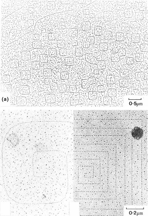
There is also a large literature devoted to such clusters at steps, including their position relative to the step, which involves long range elastic interactions in addition to other atomic level forces. The `double decoration' technique is an elegant method of demonstrating such eVects, which has been used extensively in TEM experiments over many years (Bassett 1958, Bethge 1962, Kern et al. 1979, Kern & Krohn 1989, Bethge 1990). The decoration technique is best known for demonstrating 2D island and pit nucleation, oscillatory nucleation and growth and dislocation spiral growth (and evaporation) of the alkali halides themselves, as reviewed by Mutaftschiev (1980) and Venables et al. (1984). As seen in ®gure 5.18, single height steps are rounded, double height steps square, and dislocation spirals are easily recognized.
The eVect of adatom capture by steps can be treated using an extension of (5.13) in one of two ways. Either, we can look on a scale between the steps, in which case the steps provide the boundary conditions for a rate±diVusion equation of the form
dn1/dt5R2 n1/t1-/-x(D-n1/-x). |
(5.21) |
Or, we can average over many steps, in which case adatom capture by steps adds an additional loss term to (5.13) with a characteristic time ts. We can show from the
5.5 Steps, ripening and interdiffusion |
175 |
|
|
(b) |
(c) |
Figure 5.18. Steps on KCl(001) revealed by the decoration technique: (a) single height pits;
(b) single height and (c) double height dislocation spirals (from Venables et al. 1984, reproduced with permission, after Métois et al. 1978 and Meyer & Stein 1980).

176 5 Surface processes in epitaxial growth
equivalence of these two viewpoints in complete condensation that the average adatom density n1 is
n15n1e1Rts , |
(5.22) |
|
where n1e is the concentration in equilibrium with the steps, and |
|
|
t |
5d2/12D, |
(5.23) |
s |
|
|
where d is the distance between steps; this expression is readily derived on the basis that the adatom concentration n1(x) is an inverted parabola for complete condensation, as in problem 1.4.
This simple expression may be modi®ed if evaporation, nucleation or the Ehrlich±Schwoebel (ES) barrier are allowed, as can be explored via project 5.3. The name, adopted relatively recently, stems from two papers in which the eVect was ®rst discussed (Ehrlich & Hudda 1966, Schwoebel & Shipsey 1966). TEM and FIM methods have demonstrated the ES eVect, where diVusing adatoms have diYculty in surmounting a downward step. At low temperatures the barrier is eVective, and nuclei are formed on the upper terrace right up to the down-step. An early TEM example was obtained by Klaua (1987), who observed Au ML islands decorating steps, and also nucleating on the terraces of a Ag(111) sample, as shown in ®gure 5.19.
5.5.2Steps as sources: diffusion and Ostwald ripening
Steps, in addition to being sinks, can also act as sources of adatoms. Emission of adatoms is part of sublimation, which we studied in section 1.3 via problem 1.2(b), and
in the context of adsorption in section 4.2; this happens if n1e.0 in (5.22). In this case, adatoms are created at kink sites and can diVuse over the terrace and become incorporated in other steps. When the adatom concentration is low, this process has an eVective diVusion constant
De5n1D, where n15K exp{2 (L2 Ea)/kT}, |
(5.24) |
so that the activation energy Q5(L2 Ea1Ed), with K an entropic constant. At high temperatures, other mechanisms may be active, including surface vacancies; indeed one of the diYculties of studying surface diVusion is that there are so many mechanisms which may need to be considered (Bonzel 1983, Gomer 1983, 1990, Naumovets & Vedula 1985, Naumovets 1994). However, during annealing at moderate temperatures (5.24), or a variant which allows for small amounts of clustering, is likely to be a good approximation. Such issues can be explored via project 5.4.
Noro et al. (1996) analyzed Ag patches deposited on Fe(110), following the annealing of the 3 ML of deposited Ag as shown in ®gure 5.20. The broadening of the ®rst and second ML could be followed separately, by biased secondary electron imaging as described in section 3.5; De values were deduced for Ag motion on the ®rst ML, giving an activation energy 0.86 6 0.05 eV. Using (5.24) and assuming that L for the second ML is close to the bulk Ag value of 2.95 6 0.01 eV, they found (Ea 2 Ed)52.0960.06 eV. This is to be compared with that deduced for Ag on 2 ML Ag/W(110) from the

5.5 Steps, ripening and interdiffusion |
177 |
|
|
(b)
Figure 5.19. Distribution of ML Au nuclei in relation to steps on a Ag(111) surface at the temperatures indicated. The sense of the step train corresponds to the TEM image of the Au islands. Note that the up-steps are decorated with a continuous thin strip of Au, and what is plotted is the island position histogram on the terraces, demonstrating an active ES barrier at the lower temperatures (after Klaua 1987, reproduced with permission).
nucleation experiments described in section 5.4.1: Ea52.260.1 and Ed50.1560.1eV; the values of (Ea ± Ed) are rather similar! Use of the more accurate value for Ed50.10 60.01eV from STM experiments (Brune et al. 1995, Brune 1998) makes the agreement even closer.
This type of annealing is a particular case of Ostwald ripening, which is a term usually applied to situations where large clusters grow or coarsen, and small clusters shrink or disappear. In the case of ripening controlled via adatom surface diVusion, the eVective diVusion coeYcient is given by (5.24) with activation energy Q5(L2 Ea1Ed). It is noticeable that the high temperature limit of the nucleation model in complete condensation gives this same energy, since L5Ea13Eb for large 2D (hexagonal) clusters. The nucleation density expression in table 5.1 has Ei53Eb for large critical nucleus sizes i, so the corresponding activation energy is again (Ed13Eb); this is thus an internal check on the validity of the nucleation model. Ostwald ripening is generally important in materials science (Martin & Doherty 1976, Voorhees 1985); 2D ripening on surfaces is described more fully by Zinke-Allmang et al. (1992) and Zinke-Allmang (1999).
STM experiments have been instrumental in pinning down some of these energies, and the ES barrier has been investigated speci®cally for Ag(111), where authors have

178 |
|
5 |
Surface processes in epitaxial growth |
|
|
|
|
||||
|
50 |
T = 323 +/±13 oC |
|
|
|
|
|
|
|
||
|
|
|
|
|
|
1st ML |
|
|
|
|
|
|
40 |
|
|
|
|
|
|
1E-9 |
|
|
|
|
|
|
|
|
|
|
|
|
|
|
|
m)( |
|
|
|
|
|
|
|
(cm |
|
0.81 eV |
|
|
30 |
|
|
|
|
|
|
/s) |
|
||
widthPatch |
|
|
|
|
|
|
2 |
|
|
|
|
|
|
|
|
|
|
|
D |
|
|
|
|
|
|
|
|
|
|
|
|
e |
|
|
|
|
20 |
|
|
|
|
|
|
|
|
|
|
|
|
|
|
|
|
2nd ML |
|
1E-10 |
|
|
|
|
10 |
|
|
|
|
|
|
|
|
0.88 eV |
|
|
|
|
|
islands |
|
|
|
|
|
|
|
|
|
|
|
disappear |
|
|
|
|
|
|
|
|
0 |
(a) |
|
|
|
|
|
(b) |
|
|
|
|
|
0 |
2 |
4 |
6 |
8 |
10 |
1.5 |
1.6 |
1.7 |
1.8 |
|
|
|
|
t1/2 (min1/2) |
|
|
|
1000/T (K±1) |
|
||
Figure 5.20. (a) Expansion of patches of Ag/Fe(110), initially 20 mm wide and 3ML deposited, during annealing at a typical temperature T5323613°C, the arrow indicating the time at which islands on the second ML disappear; (b) EVective diVusion coeYcient De as function of 1000/T, with activation energies Q indicated for an assumed K54 (after Noro et al. 1996, reproduced with permission). See text for discussion.
found values of ES50.1260.02 eV (Bromann et al. 1995) and 0.1360.04 eV (Morgenstern et al. 1998). This latter experiment is particularly elegant, in that the authors were able to create ML height pits on the surface by ion bombardment, and then place either islands (by deposition) or smaller ML deep pits (by further bombardment) close to the centers of the larger pits. The small pits were found to ®ll in more slowly than the islands evaporated, in annealing experiments lasting several hours around and below room temperature. This diVerence in rate is directly due to the presence of the ES barrier, whereas the average rate is governed by the same Q as above in (5.24), with Q50.7160.03 eV from the comparison of the model with experiment.
Comparison with the SEM results on Ag on 1 ML Ag/Fe(110) which gave 0.8660.05 eV is interesting, in that the SEM experiments (Noro et al. 1996) involve diVusion over a large number of steps; in this case the maximum activation energy would correspond to (Q1ES), i.e. (0.7110.13)50.84 eV, good agreement! But such arguments are at the limit of current experimental accuracy, and there are uncertainties in frequency factors, and other important eVects to consider. One which has been demonstrated is the eVect of strain, where Ag adatoms diVusing on the compressed ML phase of Ag/Pt(111) have a lower value of Ed than on Ag(111) (Ruggerone et al. 1997, Brune & Kern 1997, Brune 1998), as indicated in table 5.4. These calculations also give a lower value of ES on com-