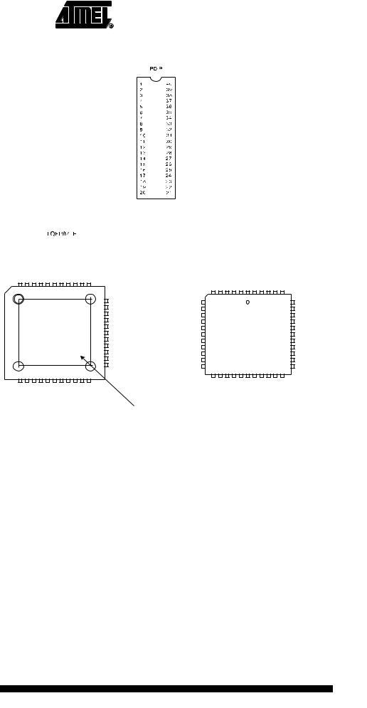
- •Features
- •Pin Configurations
- •Disclaimer
- •Overview
- •Block Diagram
- •AT90S8535 Compatibility
- •Pin Descriptions
- •Port A (PA7..PA0)
- •Port B (PB7..PB0)
- •Port C (PC7..PC0)
- •Port D (PD7..PD0)
- •RESET
- •XTAL1
- •XTAL2
- •AVCC
- •AREF
- •AVR CPU Core
- •Introduction
- •Architectural Overview
- •Status Register
- •Stack Pointer
- •Interrupt Response Time
- •SRAM Data Memory
- •Data Memory Access Times
- •EEPROM Data Memory
- •EEPROM Read/Write Access
- •I/O Memory
- •Clock Systems and their Distribution
- •Clock Sources
- •Default Clock Source
- •Crystal Oscillator
- •External RC Oscillator
- •External Clock
- •Timer/Counter Oscillator
- •Idle Mode
- •Power-down Mode
- •Power-save Mode
- •Standby Mode
- •Extended Standby Mode
- •Analog-to-Digital Converter
- •Analog Comparator
- •Brown-out Detector
- •Internal Voltage Reference
- •Watchdog Timer
- •Port Pins
- •Resetting the AVR
- •Reset Sources
- •Power-on Reset
- •External Reset
- •Brown-out Detection
- •Watchdog Reset
- •Watchdog Timer
- •Timed Sequences for Changing the Configuration of the Watchdog Timer
- •Safety Level 0
- •Safety Level 1
- •Safety Level 2
- •Interrupts
- •I/O-Ports
- •Introduction
- •Configuring the Pin
- •Reading the Pin Value
- •Unconnected pins
- •Alternate Port Functions
- •Alternate Functions of Port A
- •Alternate Functions Of Port B
- •Alternate Functions of Port C
- •Alternate Functions of Port D
- •External Interrupts
- •8-bit Timer/Counter0 with PWM
- •Overview
- •Registers
- •Definitions
- •Counter Unit
- •Output Compare Unit
- •Force Output Compare
- •Modes of Operation
- •Normal Mode
- •Fast PWM Mode
- •Phase Correct PWM Mode
- •Internal Clock Source
- •Prescaler Reset
- •External Clock Source
- •16-bit Timer/Counter1
- •Overview
- •Registers
- •Definitions
- •Compatibility
- •Counter Unit
- •Input Capture Unit
- •Input Capture Trigger Source
- •Noise Canceler
- •Using the Input Capture Unit
- •Output Compare Units
- •Force Output Compare
- •Modes of Operation
- •Normal Mode
- •Fast PWM Mode
- •Phase Correct PWM Mode
- •8-bit Timer/Counter2 with PWM and Asynchronous Operation
- •Overview
- •Registers
- •Definitions
- •Counter Unit
- •Output Compare Unit
- •Force Output Compare
- •Modes of Operation
- •Normal Mode
- •Fast PWM Mode
- •Phase Correct PWM Mode
- •Timer/Counter Prescaler
- •SS Pin Functionality
- •Slave Mode
- •Master Mode
- •Data Modes
- •USART
- •Overview
- •Clock Generation
- •External Clock
- •Synchronous Clock Operation
- •Frame Formats
- •Parity Bit Calculation
- •USART Initialization
- •Sending Frames with 5 to 8 Data Bits
- •Sending Frames with 9 Data Bits
- •Parity Generator
- •Disabling the Transmitter
- •Receiving Frames with 5 to 8 Data Bits
- •Receiving Frames with 9 Data Bits
- •Receiver Error Flags
- •Parity Checker
- •Disabling the Receiver
- •Flushing the Receive Buffer
- •Asynchronous Data Recovery
- •Using MPCM
- •Write Access
- •Read Access
- •Two-wire Serial Interface
- •Features
- •TWI Terminology
- •Electrical Interconnection
- •Transferring Bits
- •START and STOP Conditions
- •Address Packet Format
- •Data Packet Format
- •Overview of the TWI Module
- •SCL and SDA Pins
- •Bit Rate Generator Unit
- •Bus Interface Unit
- •Address Match Unit
- •Control Unit
- •TWI Register Description
- •Using the TWI
- •Transmission Modes
- •Master Transmitter Mode
- •Master Receiver Mode
- •Slave Receiver Mode
- •Slave Transmitter Mode
- •Miscellaneous States
- •Analog Comparator
- •Analog Comparator Multiplexed Input
- •Features
- •Operation
- •Starting a Conversion
- •Differential Gain Channels
- •Changing Channel or Reference Selection
- •ADC Input Channels
- •ADC Voltage Reference
- •ADC Noise Canceler
- •Analog Input Circuitry
- •ADC Accuracy Definitions
- •ADC Conversion Result
- •ADLAR = 0
- •ADLAR = 1
- •Boot Loader Features
- •Application Section
- •Boot Loader Lock Bits
- •Performing a Page Write
- •Using the SPM Interrupt
- •Setting the Boot Loader Lock Bits by SPM
- •Reading the Fuse and Lock Bits from Software
- •Preventing Flash Corruption
- •Simple Assembly Code Example for a Boot Loader
- •Fuse Bits
- •Latching of Fuses
- •Signature Bytes
- •Calibration Byte
- •Signal Names
- •Parallel Programming
- •Enter Programming Mode
- •Chip Erase
- •Programming the Flash
- •Programming the EEPROM
- •Reading the Flash
- •Reading the EEPROM
- •Programming the Lock Bits
- •Reading the Signature Bytes
- •Reading the Calibration Byte
- •Serial Downloading
- •Data Polling Flash
- •Data Polling EEPROM
- •Electrical Characteristics
- •Absolute Maximum Ratings*
- •DC Characteristics
- •External Clock Drive Waveforms
- •External Clock Drive
- •Two-wire Serial Interface Characteristics
- •Active Supply Current
- •Idle Supply Current
- •Power-Save Supply Current
- •Standby Supply Current
- •Pin Pullup
- •Pin Driver Strength
- •Internal Oscillator Speed
- •Register Summary
- •Instruction Set Summary
- •Ordering Information
- •Packaging Information
- •Errata
- •ATmega8535 all rev.
- •Datasheet Change Log for ATmega8535
- •Changes from Rev. 2502E-12/03 to Rev. 2502F-06/04
- •Changes from Rev. 2502D-09/03 to Rev. 2502E-12/03
- •Changes from Rev. 2502C-04/03 to Rev. 2502D-09/03
- •Changes from Rev. 2502B-09/02 to Rev. 2502C-04/03
- •Changes from Rev. 2502A-06/02 to Rev. 2502B-09/02
- •Table of Contents
Pin Configurations |
|
|
|
|
|
|
|
|
|
|
|
|
|
|
|
|
|
|
|
|
|
Figure 1. Pinout ATmega8535 |
|
|
||||||||
|
|
|
(XCK/T0) PB0 |
|
|
|
|
PA0 (ADC0) |
||
|
|
|
|
|
|
|
||||
|
|
|
|
|
|
|
||||
|
|
|
|
|
|
|
||||
|
|
|
|
(T1) PB1 |
|
|
|
|
PA1 (ADC1) |
|
|
|
|
|
|
|
|
|
|||
|
|
(INT2/AIN0) PB2 |
|
|
|
|
PA2 (ADC2) |
|||
|
|
|
|
|
|
|||||
|
|
(OC0/AIN1) PB3 |
|
|
|
|
PA3 (ADC3) |
|||
|
|
|
|
|
|
|||||
|
|
|
|
(SS) PB4 |
|
|
|
|
PA4 (ADC4) |
|
|
|
|
|
|
|
|
|
|||
|
|
|
|
(MOSI) PB5 |
|
|
|
|
PA5 (ADC5) |
|
|
|
|
|
|
|
|
|
|||
|
|
|
|
(MISO) PB6 |
|
|
|
|
PA6 (ADC6) |
|
|
|
|
|
|
|
|
|
|||
|
|
|
|
(SCK) PB7 |
|
|
|
|
PA7 (ADC7) |
|
|
|
|
|
|
|
|
|
|||
|
|
|
|
RESET |
|
|
|
|
AREF |
|
|
|
|
|
|
|
|
|
|||
|
|
|
|
VCC |
|
|
|
|
GND |
|
|
|
|
|
|
|
|
|
|||
|
|
|
|
GND |
|
|
|
|
AVCC |
|
|
|
|
|
XTAL2 |
|
|
|
|
PC7 (TOSC2) |
|
|
|
|
|
XTAL1 |
|
|
|
|
PC6 (TOSC1) |
|
|
|
|
|
(RXD) PD0 |
|
|
|
|
PC5 |
|
|
|
|
|
(TXD) PD1 |
|
|
|
|
PC4 |
|
|
|
|
|
(INT0) PD2 |
|
|
|
|
PC3 |
|
|
|
|
|
(INT1) PD3 |
|
|
|
|
PC2 |
|
|
|
|
|
(OC1B) PD4 |
|
|
|
|
PC1 (SDA) |
|
|
|
|
|
(OC1A) PD5 |
|
|
|
|
PC0 (SCL) |
|
|
|
|
|
(ICP1) PD6 |
|
|
|
|
PD7 (OC2) |
(MOSI) PB5 1 (MISO) PB6 2 (SCK) PB7 3 RESET 4 VCC 5 GND 6 XTAL2 7 XTAL1 8
(RXD) PD0 9 (TXD) PD1 10 (INT0) PD2 11
|
|
|
|
|
|
|
|
|
|
|
|
|
|
|
|
|
PLCC |
|
|
|
|
|||
44 PB4 (SS) |
43 PB3 (AIN1/OC0) |
42 PB2 (AIN0/INT2) |
41 PB1 (T1) |
40 PB0 (XCK/T0) |
39 GND |
38 VCC |
37 PA0 (ADC0) |
36 PA1 (ADC1) |
35 PA2 (ADC2) |
34 PA3 (ADC3) |
|
|
PB4 (SS) |
PB3 (AIN1/OC0) |
PB2 (AIN0/INT2) |
PB1 (T1) |
PB0 (XCK/T0) |
GND |
VCC |
PA0 (ADC0) |
PA1 (ADC1) |
PA2 (ADC2) |
PA3 (ADC3) |
|
|
|
|
|
|
|
|
|
|
|
33 |
PA4 (ADC4) |
(MOSI) PB5 |
6 |
5 |
4 |
3 |
2 |
1 |
44 |
43 |
42 |
41 |
40 |
PA4 (ADC4) |
|
|
|
|
|
|
|
|
|
|
7 |
|
|
|
|
|
|
|
|
|
39 |
||||
|
|
|
|
|
|
|
|
|
|
32 |
PA5 (ADC5) |
(MISO) PB6 |
8 |
|
|
|
|
|
|
|
|
|
38 |
PA5 (ADC5) |
|
|
|
|
|
|
|
|
|
|
31 |
PA6 (ADC6) |
(SCK) PB7 |
9 |
|
|
|
|
|
|
|
|
|
37 |
PA6 (ADC6) |
|
|
|
|
|
|
|
|
|
|
30 |
PA7 (ADC7) |
RESET |
10 |
|
|
|
|
|
|
|
|
|
36 |
PA7 (ADC7) |
|
|
|
|
|
|
|
|
|
|
29 |
AREF |
VCC |
11 |
|
|
|
|
|
|
|
|
|
35 |
AREF |
|
|
|
|
|
|
|
|
|
|
28 |
GND |
GND |
12 |
|
|
|
|
|
|
|
|
|
34 |
GND |
|
|
|
|
|
|
|
|
|
|
27 |
AVCC |
XTAL2 |
13 |
|
|
|
|
|
|
|
|
|
33 |
AVCC |
|
|
|
|
|
|
|
|
|
|
26 |
PC7 (TOSC2) |
XTAL1 |
14 |
|
|
|
|
|
|
|
|
|
32 |
PC7 (TOSC2) |
|
|
|
|
|
|
|
|
|
|
25 |
PC6 (TOSC1) |
(RXD) PD0 |
15 |
|
|
|
|
|
|
|
|
|
31 |
PC6 (TOSC1) |
|
|
|
|
|
|
|
|
|
|
24 |
PC5 |
(TXD) PD1 |
16 |
|
|
|
|
|
|
|
|
|
30 |
PC5 |
|
|
|
|
|
|
|
|
|
|
23 |
PC4 |
(INT0) PD2 |
17 |
19 |
20 |
21 |
22 |
23 |
24 |
25 |
26 |
27 |
29 |
PC4 |
12 |
13 |
14 |
15 |
16 |
17 |
18 |
19 |
20 |
21 |
22 |
|
|
18 |
28 |
|
|||||||||
|
|
(INT1) PD3 |
(OC1B) PD4 |
(OC1A) PD5 |
(ICP1) PD6 |
(OC2) PD7 |
VCC |
GND |
(SCL) PC0 |
(SDA) PC1 |
PC2 |
PC3 |
|
|||||||||||
(INT1) PD3 |
(OC1B) PD4 |
(OC1A) PD5 |
(ICP1) PD6 |
(OC2) PD7 |
VCC |
GND |
(SCL) PC0 |
(SDA) PC1 |
PC2 |
PC3 |
|
|
|
NOTE: MLF Bottom pad should be soldered to ground.
Disclaimer |
Typical values contained in this data sheet are based on simulations and characteriza- |
|
tion of other AVR microcontrollers manufactured on the same process technology. Min |
|
and Max values will be available after the device is characterized. |
2 ATmega8535(L)
2502F–AVR–06/04