

- •Features
- •Pin Configurations
- •Disclaimer
- •Overview
- •Block Diagram
- •AT90S8535 Compatibility
- •Pin Descriptions
- •Port A (PA7..PA0)
- •Port B (PB7..PB0)
- •Port C (PC7..PC0)
- •Port D (PD7..PD0)
- •RESET
- •XTAL1
- •XTAL2
- •AVCC
- •AREF
- •AVR CPU Core
- •Introduction
- •Architectural Overview
- •Status Register
- •Stack Pointer
- •Interrupt Response Time
- •SRAM Data Memory
- •Data Memory Access Times
- •EEPROM Data Memory
- •EEPROM Read/Write Access
- •I/O Memory
- •Clock Systems and their Distribution
- •Clock Sources
- •Default Clock Source
- •Crystal Oscillator
- •External RC Oscillator
- •External Clock
- •Timer/Counter Oscillator
- •Idle Mode
- •Power-down Mode
- •Power-save Mode
- •Standby Mode
- •Extended Standby Mode
- •Analog-to-Digital Converter
- •Analog Comparator
- •Brown-out Detector
- •Internal Voltage Reference
- •Watchdog Timer
- •Port Pins
- •Resetting the AVR
- •Reset Sources
- •Power-on Reset
- •External Reset
- •Brown-out Detection
- •Watchdog Reset
- •Watchdog Timer
- •Timed Sequences for Changing the Configuration of the Watchdog Timer
- •Safety Level 0
- •Safety Level 1
- •Safety Level 2
- •Interrupts
- •I/O-Ports
- •Introduction
- •Configuring the Pin
- •Reading the Pin Value
- •Unconnected pins
- •Alternate Port Functions
- •Alternate Functions of Port A
- •Alternate Functions Of Port B
- •Alternate Functions of Port C
- •Alternate Functions of Port D
- •External Interrupts
- •8-bit Timer/Counter0 with PWM
- •Overview
- •Registers
- •Definitions
- •Counter Unit
- •Output Compare Unit
- •Force Output Compare
- •Modes of Operation
- •Normal Mode
- •Fast PWM Mode
- •Phase Correct PWM Mode
- •Internal Clock Source
- •Prescaler Reset
- •External Clock Source
- •16-bit Timer/Counter1
- •Overview
- •Registers
- •Definitions
- •Compatibility
- •Counter Unit
- •Input Capture Unit
- •Input Capture Trigger Source
- •Noise Canceler
- •Using the Input Capture Unit
- •Output Compare Units
- •Force Output Compare
- •Modes of Operation
- •Normal Mode
- •Fast PWM Mode
- •Phase Correct PWM Mode
- •8-bit Timer/Counter2 with PWM and Asynchronous Operation
- •Overview
- •Registers
- •Definitions
- •Counter Unit
- •Output Compare Unit
- •Force Output Compare
- •Modes of Operation
- •Normal Mode
- •Fast PWM Mode
- •Phase Correct PWM Mode
- •Timer/Counter Prescaler
- •SS Pin Functionality
- •Slave Mode
- •Master Mode
- •Data Modes
- •USART
- •Overview
- •Clock Generation
- •External Clock
- •Synchronous Clock Operation
- •Frame Formats
- •Parity Bit Calculation
- •USART Initialization
- •Sending Frames with 5 to 8 Data Bits
- •Sending Frames with 9 Data Bits
- •Parity Generator
- •Disabling the Transmitter
- •Receiving Frames with 5 to 8 Data Bits
- •Receiving Frames with 9 Data Bits
- •Receiver Error Flags
- •Parity Checker
- •Disabling the Receiver
- •Flushing the Receive Buffer
- •Asynchronous Data Recovery
- •Using MPCM
- •Write Access
- •Read Access
- •Two-wire Serial Interface
- •Features
- •TWI Terminology
- •Electrical Interconnection
- •Transferring Bits
- •START and STOP Conditions
- •Address Packet Format
- •Data Packet Format
- •Overview of the TWI Module
- •SCL and SDA Pins
- •Bit Rate Generator Unit
- •Bus Interface Unit
- •Address Match Unit
- •Control Unit
- •TWI Register Description
- •Using the TWI
- •Transmission Modes
- •Master Transmitter Mode
- •Master Receiver Mode
- •Slave Receiver Mode
- •Slave Transmitter Mode
- •Miscellaneous States
- •Analog Comparator
- •Analog Comparator Multiplexed Input
- •Features
- •Operation
- •Starting a Conversion
- •Differential Gain Channels
- •Changing Channel or Reference Selection
- •ADC Input Channels
- •ADC Voltage Reference
- •ADC Noise Canceler
- •Analog Input Circuitry
- •ADC Accuracy Definitions
- •ADC Conversion Result
- •ADLAR = 0
- •ADLAR = 1
- •Boot Loader Features
- •Application Section
- •Boot Loader Lock Bits
- •Performing a Page Write
- •Using the SPM Interrupt
- •Setting the Boot Loader Lock Bits by SPM
- •Reading the Fuse and Lock Bits from Software
- •Preventing Flash Corruption
- •Simple Assembly Code Example for a Boot Loader
- •Fuse Bits
- •Latching of Fuses
- •Signature Bytes
- •Calibration Byte
- •Signal Names
- •Parallel Programming
- •Enter Programming Mode
- •Chip Erase
- •Programming the Flash
- •Programming the EEPROM
- •Reading the Flash
- •Reading the EEPROM
- •Programming the Lock Bits
- •Reading the Signature Bytes
- •Reading the Calibration Byte
- •Serial Downloading
- •Data Polling Flash
- •Data Polling EEPROM
- •Electrical Characteristics
- •Absolute Maximum Ratings*
- •DC Characteristics
- •External Clock Drive Waveforms
- •External Clock Drive
- •Two-wire Serial Interface Characteristics
- •Active Supply Current
- •Idle Supply Current
- •Power-Save Supply Current
- •Standby Supply Current
- •Pin Pullup
- •Pin Driver Strength
- •Internal Oscillator Speed
- •Register Summary
- •Instruction Set Summary
- •Ordering Information
- •Packaging Information
- •Errata
- •ATmega8535 all rev.
- •Datasheet Change Log for ATmega8535
- •Changes from Rev. 2502E-12/03 to Rev. 2502F-06/04
- •Changes from Rev. 2502D-09/03 to Rev. 2502E-12/03
- •Changes from Rev. 2502C-04/03 to Rev. 2502D-09/03
- •Changes from Rev. 2502B-09/02 to Rev. 2502C-04/03
- •Changes from Rev. 2502A-06/02 to Rev. 2502B-09/02
- •Table of Contents

Figure 98. Analog-to-Digital Converter Block Schematic
ADC CONVERSION
COMPLETE IRQ
|
|
|
|
|
|
INTERRUPT |
|
|
|
|
|
|
|
|
FLAGS |
|
|
|
|
|
|
|
|
ADTS[2:0] |
|
|
|
|
|
|
|
|
|
||
8-BIT DATA BUS |
|
|
|
|
|
|
|
|
|
|
|
ADIF |
ADIE |
|
15 |
|
0 |
|
|
|
|
|
||||
ADC MULTIPLEXER |
|
|||||||
ADC CTRL. & STATUS |
ADC DATA REGISTER |
|
||||||
SELECT (ADMUX) |
REGISTER (ADCSRA) |
(ADCH/ADCL) |
|
|||||
REFS1 |
REFS0 |
ADLAR |
MUX4 |
MUX3 |
MUX2 |
MUX1 |
MUX0 |
ADEN |
ADSC |
ADATE |
ADIF |
ADPS2 |
ADPS1 |
ADPS0 |
TRIGGER |
ADC[9:0] |
|
|
|
|
|
|
|
|
|
|
|
|
|
|
|
SELECT |
|
MUX DECODER
|
CHANNEL SELECTION |
|
PRESCALER |
|
GAIN SELECTION |
START |
|
AVCC |
CONVERSION LOGIC |
||
|
|||
|
|
||
|
INTERNAL 2.56V |
|
|
|
REFERENCE |
|
SAMPLE & HOLD |
|
|
|
COMPARATOR |
AREF |
|
10-BIT DAC |
- |
|
|
||
|
|
|
+ |
GND |
|
|
|
|
BANDGAP |
|
|
|
REFERENCE |
|
|
ADC7 |
|
|
|
|
|
SINGLE ENDED / DIFFERENTIAL SELECTION |
|
ADC6 |
|
|
|
ADC5 |
POS. |
|
ADC MULTIPLEXER |
INPUT |
|
OUTPUT |
|
|
|
||
|
MUX |
|
|
ADC4 |
|
|
|
ADC3 |
|
GAIN |
|
|
|
AMPLIFIER |
|
ADC2 |
|
+ |
|
|
|
|
|
|
|
- |
|
ADC1 |
|
|
|
ADC0 |
|
|
|
|
NEG. |
|
|
|
INPUT |
|
|
|
MUX |
|
|
Operation |
The ADC converts an analog input voltage to a 10-bit digital value through successive |
|
approximation. The minimum value represents GND and the maximum value represents |
|
the voltage on the AREF pin minus 1 LSB. Optionally, AVCC or an internal 2.56V refer- |
|
ence voltage may be connected to the AREF pin by writing to the REFSn bits in the |
|
ADMUX Register. The internal voltage reference may thus be decoupled by an external |
|
capacitor at the AREF pin to improve noise immunity. |
|
The analog input channel and differential gain are selected by writing to the MUX bits in |
|
ADMUX. Any of the ADC input pins, as well as GND and a fixed bandgap voltage refer- |
|
ence, can be selected as single ended inputs to the ADC. A selection of ADC input pins |
|
can be selected as positive and negative inputs to the differential gain amplifier. |
|
If differential channels are selected, the differential gain stage amplifies the voltage dif- |
|
ference between the selected input channel pair by the selected gain factor. This |
|
amplified value then becomes the analog input to the ADC. If single ended channels are |
|
used, the gain amplifier is bypassed altogether. |
204 ATmega8535(L)
2502F–AVR–06/04

 ATmega8535(L)
Starting a Conversion
The ADC is enabled by setting the ADC Enable bit, ADEN in ADCSRA. Voltage reference and input channel selections will not go into effect until ADEN is set. The ADC does not consume power when ADEN is cleared, so it is recommended to switch off the ADC before entering power saving sleep modes.
The ADC generates a 10-bit result which is presented in the ADC Data Registers, ADCH and ADCL. By default, the result is presented right adjusted, but can optionally be presented left adjusted by setting the ADLAR bit in ADMUX.
If the result is left adjusted and no more than 8-bit precision is required, it is sufficient to read ADCH. Otherwise, ADCL must be read first, then ADCH, to ensure that the content of the data registers belongs to the same conversion. Once ADCL is read, ADC access to data registers is blocked. This means that if ADCL has been read, and a conversion completes before ADCH is read, neither register is updated and the result from the conversion is lost. When ADCH is read, ADC access to the ADCH and ADCL Registers is re-enabled.
The ADC has its own interrupt which can be triggered when a conversion completes. When ADC access to the data registers is prohibited between reading of ADCH and ADCL, the interrupt will trigger even if the result is lost.
A single conversion is started by writing a logical one to the ADC Start Conversion bit, ADSC. This bit stays high as long as the conversion is in progress and will be cleared by hardware when the conversion is completed. If a different data channel is selected while a conversion is in progress, the ADC will finish the current conversion before performing the channel change.
Alternatively, a conversion can be triggered automatically by various sources. Auto Triggering is enabled by setting the ADC Auto Trigger Enable bit, ADATE in ADCSRA. The trigger source is selected by setting the ADC Trigger Select bits, ADTS in SFIOR (See description of the ADTS bits for a list of the trigger sources). When a positive edge occurs on the selected trigger signal, the ADC prescaler is reset and a conversion is started. This provides a method of starting conversions at fixed intervals. If the trigger signal still is set when the conversion completes, a new conversion will not be started. If another positive edge occurs on the trigger signal during conversion, the edge will be ignored. Note that an interrupt flag will be set even if the specific interrupt is disabled or the global interrupt enable bit in SREG is cleared. A conversion can thus be triggered without causing an interrupt. However, the interrupt flag must be cleared in order to trigger a new conversion at the next interrupt event.
205
2502F–AVR–06/04

Prescaling and
Conversion Timing
Figure 99. ADC Auto Trigger Logic
|
ADTS[2:0] |
PRESCALER |
|
|
|
|
START |
CLKADC |
ADIF |
ADATE |
|
SOURCE 1 |
|
|
. |
|
CONVERSION |
. |
|
|
|
LOGIC |
|
. |
|
|
|
|
|
. |
EDGE |
|
SOURCE n |
DETECTOR |
|
|
|
ADSC
Using the ADC Interrupt Flag as a trigger source makes the ADC start a new conversion as soon as the ongoing conversion has finished. The ADC then operates in Free Running mode, constantly sampling and updating the ADC Data Register. The first conversion must be started by writing a logical one to the ADSC bit in ADCSRA. In this mode the ADC will perform successive conversions independently of whether the ADC Interrupt Flag, ADIF is cleared or not.
If Auto Triggering is enabled, single conversions can be started by writing ADSC in ADCSRA to one. ADSC can also be used to determine if a conversion is in progress. The ADSC bit will be read as one during a conversion, independently of how the conversion was started.
Figure 100. ADC Prescaler
ADEN |
Reset |
|
START |
||
|
7-BIT ADC PRESCALER
CK 
CK/2 |
CK/4 |
CK/8 |
CK/16 |
CK/32 |
CK/64 |
CK/128 |
ADPS0
ADPS1
ADPS2
ADC CLOCK SOURCE
By default, the successive approximation circuitry requires an input clock frequency between 50 kHz and 200 kHz to get maximum resolution. If a lower resolution than 10 bits is needed, the input clock frequency to the ADC can be higher than 200 kHz to get a higher sample rate.
206 ATmega8535(L)
2502F–AVR–06/04

 ATmega8535(L)
The ADC module contains a prescaler, which generates an acceptable ADC clock frequency from any CPU frequency above 100 kHz. The prescaling is set by the ADPS bits in ADCSRA. The prescaler starts counting from the moment the ADC is switched on by setting the ADEN bit in ADCSRA. The prescaler keeps running for as long as the ADEN bit is set, and is continuously reset when ADEN is low.
When initiating a single ended conversion by setting the ADSC bit in ADCSRA, the conversion starts at the following rising edge of the ADC clock cycle. See “Differential Gain Channels” on page 209 for details on differential conversion timing.
A normal conversion takes 13 ADC clock cycles. The first conversion after the ADC is switched on (ADEN in ADCSRA is set) takes 25 ADC clock cycles in order to initialize the analog circuitry.
The actual sample-and-hold takes place 1.5 ADC clock cycles after the start of a normal conversion and 13.5 ADC clock cycles after the start of an first conversion. When a conversion is complete, the result is written to the ADC Data Registers, and ADIF is set. In Single Conversion mode, ADSC is cleared simultaneously. The software may then set ADSC again, and a new conversion will be initiated on the first rising ADC clock edge.
When Auto Triggering is used, the prescaler is reset when the trigger event occurs. This assures a fixed delay from the trigger event to the start of conversion. In this mode, the sample-and-hold takes place two ADC clock cycles after the rising edge on the trigger source signal. Three additional CPU clock cycles are used for synchronization logic.
In Free Running mode, a new conversion will be started immediately after the conversion completes, while ADSC remains high. For a summary of conversion times, see Table 82.
Figure 101. ADC Timing Diagram, First Conversion (Single Conversion Mode)
|
|
|
|
First Conversion |
|
Next |
|
|
|
|
|
|
|
Conversion |
|||
|
|
|
|
|
|
|||
Cycle Number |
1 |
2 |
12 13 |
14 15 16 17 18 19 20 21 22 23 24 25 |
1 |
2 |
3 |
|
ADC Clock |
|
|
|
|
|
|
|
|
ADEN |
|
|
|
|
|
|
|
|
ADSC |
|
|
|
|
|
|
|
|
ADIF |
|
|
|
|
|
|
|
|
ADCH |
|
|
|
|
|
MSB of Result |
|
|
|
|
|
|
|
|
|
|
|
ADCL |
|
|
|
|
|
LSB of Result |
||
|
|
|
|
|
|
|
|
|
|
|
|
MUX and REFS |
Sample & Hold |
Conversion |
|
|
MUX and REFS |
|
|
|
Update |
Complete |
|
|
Update |
|
|
|
|
|
|
|
|||
207
2502F–AVR–06/04
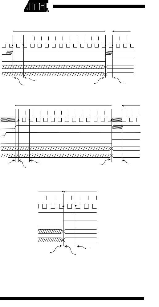
Figure 102. ADC Timing Diagram, Single Conversion
|
|
|
|
|
|
|
|
One Conversion |
|
Next Conversion |
|||
Cycle Number |
1 |
2 |
3 |
4 |
5 |
6 |
7 |
8 |
9 |
10 11 12 13 |
1 |
2 |
3 |
ADC Clock |
|
|
|
|
|
|
|
|
|
|
|
|
|
ADSC |
|
|
|
|
|
|
|
|
|
|
|
|
|
ADIF |
|
|
|
|
|
|
|
|
|
|
|
|
|
ADCH |
|
|
|
|
|
|
|
|
|
|
MSB of Result |
|
|
ADCL |
|
|
|
|
|
|
|
|
|
|
LSB of Result |
|
|
|
|
|
|
Sample & Hold |
|
|
|
|
Conversion |
|
MUX and REFS |
||
|
|
MUX and REFS |
|
|
|
|
|
|
|||||
|
|
|
|
|
|
|
Complete |
|
Update |
||||
|
|
Update |
|
|
|
|
|
|
|
|
|
|
|
Figure 103. ADC Timing Diagram, Auto Triggered Conversion
|
|
|
|
|
|
|
|
One Conversion |
|
|
|
|
Next Conversion |
||
Cycle Number |
1 |
2 |
3 |
4 |
5 |
6 |
7 |
8 |
9 |
10 |
11 |
12 |
13 |
1 |
2 |
ADC Clock |
|
|
|
|
|
|
|
|
|
|
|
|
|
|
|
Trigger |
|
|
|
|
|
|
|
|
|
|
|
|
|
|
|
Source |
|
|
|
|
|
|
|
|
|
|
|
|
|
|
|
ADATE |
|
|
|
|
|
|
|
|
|
|
|
|
|
|
|
ADIF |
|
|
|
|
|
|
|
|
|
|
|
|
|
|
|
ADCH |
|
|
|
|
|
|
|
|
|
|
|
|
|
MSB of Result |
|
ADCL |
|
|
|
|
|
|
|
|
|
|
|
|
|
LSB of Result |
|
Prescaler |
|
|
|
Sample & |
|
|
|
|
|
Conversion |
|
|
Prescaler |
||
|
|
|
Hold |
|
|
|
|
|
Complete |
|
|
Reset |
|
||
Reset |
|
|
|
|
|
|
|
|
|
|
|
||||
MUX and REFS |
|
|
|
|
|
|
|
|
|
|
|
|
|
||
|
|
|
|
|
|
|
|
|
|
|
|
|
|
||
|
Update |
|
|
|
|
|
|
|
|
|
|
|
|
|
|
Figure 104. ADC Timing Diagram, Free Running Conversion
|
One Conversion |
|
Next Conversion |
|
|||
Cycle Number |
11 |
12 |
13 |
1 |
2 |
3 |
4 |
|
|
|
|
|
|
|
|
ADC Clock |
|
|
|
|
|
|
|
ADSC |
|
|
|
|
|
|
|
ADIF |
|
|
|
|
|
|
|
ADCH |
|
|
|
MSB of Result |
|
||
ADCL |
|
|
|
LSB of Result |
|
||
Conversion |
|
|
|
|
|
Sample & Hold |
|
|
|
|
|
|
|
||
Complete |
|
|
|
MUX and REFS |
|||
|
|
|
|
|
Update |
|
|
208 ATmega8535(L)
2502F–AVR–06/04