

- •Features
- •Disclaimer
- •Overview
- •Block Diagram
- •Pin Descriptions
- •Port A (PA7..PA0)
- •Port B (PB7..PB0)
- •Port C (PC7..PC0)
- •Port D (PD7..PD0)
- •RESET
- •XTAL1
- •XTAL2
- •AVCC
- •AREF
- •Resources
- •Data Retention
- •AVR CPU Core
- •Introduction
- •Status Register
- •Stack Pointer
- •I/O Memory
- •Clock Systems and their Distribution
- •Clock Sources
- •Crystal Oscillator
- •External Clock
- •Idle Mode
- •Power-down Mode
- •Power-save Mode
- •Standby Mode
- •Analog Comparator
- •Brown-out Detector
- •Watchdog Timer
- •Port Pins
- •Resetting the AVR
- •Reset Sources
- •Power-on Reset
- •External Reset
- •Watchdog Reset
- •Watchdog Timer
- •Interrupts
- •I/O Ports
- •Introduction
- •Configuring the Pin
- •Reading the Pin Value
- •Unconnected pins
- •Alternate Port Functions
- •Register Description for I/O Ports
- •8-bit Timer/Counter0 with PWM
- •Overview
- •Registers
- •Definitions
- •Counter Unit
- •Normal Mode
- •Fast PWM Mode
- •8-bit Timer/Counter Register Description
- •Timer/Counter0 and Timer/Counter1 Prescalers
- •Internal Clock Source
- •Prescaler Reset
- •External Clock Source
- •16-bit Timer/Counter1
- •Overview
- •Registers
- •Definitions
- •Compatibility
- •Counter Unit
- •Input Capture Unit
- •Noise Canceler
- •Force Output Compare
- •Normal Mode
- •Fast PWM Mode
- •16-bit Timer/Counter Register Description
- •8-bit Timer/Counter2 with PWM and Asynchronous Operation
- •Overview
- •Registers
- •Definitions
- •Counter Unit
- •Normal Mode
- •Fast PWM Mode
- •8-bit Timer/Counter Register Description
- •Slave Mode
- •Master Mode
- •Data Modes
- •USART
- •Overview
- •Clock Generation
- •External Clock
- •Frame Formats
- •Parity Bit Calculation
- •Parity Generator
- •Receiver Error Flags
- •Parity Checker
- •Disabling the Receiver
- •Using MPCM
- •Write Access
- •Read Access
- •Features
- •TWI Terminology
- •Transferring Bits
- •Address Packet Format
- •Data Packet Format
- •Overview of the TWI Module
- •SCL and SDA Pins
- •Bus Interface Unit
- •Address Match Unit
- •Control Unit
- •Using the TWI
- •Master Receiver Mode
- •Slave Receiver Mode
- •Miscellaneous States
- •Analog Comparator Multiplexed Input
- •Analog to Digital Converter
- •Features
- •Operation
- •Changing Channel or Reference Selection
- •ADC Input Channels
- •Analog Input Circuitry
- •Features
- •Overview
- •TAP Controller
- •PRIVATE0; $8
- •PRIVATE1; $9
- •PRIVATE2; $A
- •PRIVATE3; $B
- •Bibliography
- •IEEE 1149.1 (JTAG) Boundary-scan
- •Features
- •System Overview
- •Data Registers
- •Bypass Register
- •Reset Register
- •EXTEST; $0
- •IDCODE; $1
- •AVR_RESET; $C
- •BYPASS; $F
- •Scanning the ADC
- •ATmega16 Boundary-scan Order
- •Features
- •Application Section
- •Read-While-Write and no Read- While-Write Flash Sections
- •Prevent Reading the RWW Section during Self-Programming
- •Simple Assembly Code Example for a Boot Loader
- •Fuse Bits
- •Latching of Fuses
- •Signature Bytes
- •Calibration Byte
- •Page Size
- •Signal Names
- •Chip Erase
- •Reading the Flash
- •Reading the EEPROM
- •Data Polling Flash
- •Data Polling EEPROM
- •AVR_RESET ($C)
- •PROG_ENABLE ($4)
- •Data Registers
- •Reset Register
- •Programming Enable Register
- •Programming Command Register
- •Virtual Flash Page Read Register
- •Performing Chip Erase
- •Reading the Flash
- •Reading the EEPROM
- •Electrical Characteristics
- •Absolute Maximum Ratings*
- •DC Characteristics
- •External Clock Drive Waveforms
- •External Clock Drive
- •Two-wire Serial Interface Characteristics
- •ADC Characteristics
- •Idle Supply Current
- •Pin Pullup
- •Pin Driver Strength
- •Register Summary
- •Instruction Set Summary
- •Ordering Information
- •Packaging Information
- •Errata

Changing Channel or Reference Selection
single conversions, and the first free running conversion) when CKADC2 is low will take the same amount of time as a single ended conversion (13 ADC clock cycles from the next prescaled
clock cycle). A conversion initiated by the user when CKADC2 is high will take 14 ADC clock cycles due to the synchronization mechanism. In Free Running mode, a new conversion is initi-
ated immediately after the previous conversion completes, and since CKADC2 is high at this time, all automatically started (i.e., all but the first) free running conversions will take 14 ADC clock cycles.
The gain stage is optimized for a bandwidth of 4 kHz at all gain settings. Higher frequencies may be subjected to non-linear amplification. An external low-pass filter should be used if the input signal contains higher frequency components than the gain stage bandwidth. Note that the ADC clock frequency is independent of the gain stage bandwidth limitation. For example, the ADC clock period may be 6 µs, allowing a channel to be sampled at 12 kSPS, regardless of the bandwidth of this channel.
If differential gain channels are used and conversions are started by Auto Triggering, the ADC must be switched off between conversions. When Auto Triggering is used, the ADC prescaler is reset before the conversion is started. Since the gain stage is dependent of a stable ADC clock prior to the conversion, this conversion will not be valid. By disabling and then re-enabling the ADC between each conversion (writing ADEN in ADCSRA to “0” then to “1”), only extended conversions are performed. The result from the extended conversions will be valid. See “Prescaling and Conversion Timing” on page 207 for timing details.
The MUXn and REFS1:0 bits in the ADMUX Register are single buffered through a temporary register to which the CPU has random access. This ensures that the channels and reference selection only takes place at a safe point during the conversion. The channel and reference selection is continuously updated until a conversion is started. Once the conversion starts, the channel and reference selection is locked to ensure a sufficient sampling time for the ADC. Continuous updating resumes in the last ADC clock cycle before the conversion completes (ADIF in ADCSRA is set). Note that the conversion starts on the following rising ADC clock edge after ADSC is written. The user is thus advised not to write new channel or reference selection values to ADMUX until one ADC clock cycle after ADSC is written.
If Auto Triggering is used, the exact time of the triggering event can be indeterministic. Special care must be taken when updating the ADMUX Register, in order to control which conversion will be affected by the new settings.
If both ADATE and ADEN is written to one, an interrupt event can occur at any time. If the ADMUX Register is changed in this period, the user cannot tell if the next conversion is based on the old or the new settings. ADMUX can be safely updated in the following ways:
1.When ADATE or ADEN is cleared.
2.During conversion, minimum one ADC clock cycle after the trigger event.
3.After a conversion, before the Interrupt Flag used as trigger source is cleared.
When updating ADMUX in one of these conditions, the new settings will affect the next ADC conversion.
Special care should be taken when changing differential channels. Once a differential channel has been selected, the gain stage may take as much as 125 µs to stabilize to the new value. Thus conversions should not be started within the first 125 µs after selecting a new differential channel. Alternatively, conversion results obtained within this period should be discarded.
The same settling time should be observed for the first differential conversion after changing ADC reference (by changing the REFS1:0 bits in ADMUX).
210 ATmega16(L)
2466P–AVR–08/07
 ATmega16(L)
ADC Input Channels |
When changing channel selections, the user should observe the following guidelines to ensure |
||||
|
that the correct channel is selected: |
||||
|
In Single Conversion mode, always select the channel before starting the conversion. The chan- |
||||
|
nel selection may be changed one ADC clock cycle after writing one to ADSC. However, the |
||||
|
simplest method is to wait for the conversion to complete before changing the channel selection. |
||||
|
In Free Running mode, always select the channel before starting the first conversion. The chan- |
||||
|
nel selection may be changed one ADC clock cycle after writing one to ADSC. However, the |
||||
|
simplest method is to wait for the first conversion to complete, and then change the channel |
||||
|
selection. Since the next conversion has already started automatically, the next result will reflect |
||||
|
the previous channel selection. Subsequent conversions will reflect the new channel selection. |
||||
|
When switching to a differential gain channel, the first conversion result may have a poor accu- |
||||
|
racy due to the required settling time for the automatic offset cancellation circuitry. The user |
||||
|
should preferably disregard the first conversion result. |
||||
ADC Voltage |
The reference voltage for the ADC (VREF) indicates the conversion range for the ADC. Single |
||||
Reference |
ended channels that exceed VREF will result in codes close to 0x3FF. VREF can be selected as |
||||
|
either AVCC, internal 2.56V reference, or external AREF pin. |
||||
|
AVCC is connected to the ADC through a passive switch. The internal 2.56V reference is gener- |
||||
|
ated from the internal bandgap reference (VBG) through an internal amplifier. In either case, the |
||||
|
external AREF pin is directly connected to the ADC, and the reference voltage can be made |
||||
|
more immune to noise by connecting a capacitor between the AREF pin and ground. VREF can |
||||
|
also be measured at the AREF pin with a high impedant voltmeter. Note that VREF is a high |
||||
|
impedant source, and only a capacitive load should be connected in a system. |
||||
|
If the user has a fixed voltage source connected to the AREF pin, the user may not use the other |
||||
|
reference voltage options in the application, as they will be shorted to the external voltage. If no |
||||
|
external voltage is applied to the AREF pin, the user may switch between AVCC and 2.56V as |
||||
|
reference selection. The first ADC conversion result after switching reference voltage source |
||||
|
may be inaccurate, and the user is advised to discard this result. |
||||
|
If differential channels are used, the selected reference should not be closer to AVCC than |
||||
|
indicated in Table 122 on page 297. |
||||
ADC Noise |
The ADC features a noise canceler that enables conversion during sleep mode to reduce noise |
||||
Canceler |
induced from the CPU core and other I/O peripherals. The noise canceler can be used with ADC |
||||
|
Noise Reduction and Idle mode. To make use of this feature, the following procedure should be |
||||
|
used: |
||||
|
1. Make sure that the ADC is enabled and is not busy converting. Single Conversion |
||||
|
Mode must be selected and the ADC conversion complete interrupt must be |
||||
|
enabled. |
||||
|
2. Enter ADC Noise Reduction mode (or Idle mode). The ADC will start a conversion |
||||
|
once the CPU has been halted. |
||||
|
3. If no other interrupts occur before the ADC conversion completes, the ADC interrupt |
||||
|
will wake up the CPU and execute the ADC Conversion Complete interrupt routine. If |
||||
|
another interrupt wakes up the CPU before the ADC conversion is complete, that |
||||
|
interrupt will be executed, and an ADC Conversion Complete interrupt request will be |
||||
|
generated when the ADC conversion completes. The CPU will remain in active mode |
||||
|
until a new sleep command is executed. |
||||
|
Note that the ADC will not be automatically turned off when entering other sleep modes than Idle |
||||
|
mode and ADC Noise Reduction mode. The user is advised to write zero to ADEN before enter- |
||||
|
ing such sleep modes to avoid excessive power consumption. If the ADC is enabled in such |
||||
|
|
|
|
|
|
|
|
|
|
|
211 |
|
|
|
|
|
|
|
|
|
|
|
|
2466P–AVR–08/07

sleep modes and the user wants to perform differential conversions, the user is advised to switch the ADC off and on after waking up from sleep to prompt an extended conversion to get a valid result.
Analog Input Circuitry The Analog Input Circuitry for single ended channels is illustrated in Figure 105. An analog source applied to ADCn is subjected to the pin capacitance and input leakage of that pin, regardless of whether that channel is selected as input for the ADC. When the channel is selected, the source must drive the S/H capacitor through the series resistance (combined resistance in the input path).
The ADC is optimized for analog signals with an output impedance of approximately 10 kΩ or less. If such a source is used, the sampling time will be negligible. If a source with higher impedance is used, the sampling time will depend on how long time the source needs to charge the S/H capacitor, with can vary widely. The user is recommended to only use low impedant sources with slowly varying signals, since this minimizes the required charge transfer to the S/H capacitor.
If differential gain channels are used, the input circuitry looks somewhat different, although source impedances of a few hundred kΩ or less is recommended.
Signal components higher than the Nyquist frequency (fADC/2) should not be present for either kind of channels, to avoid distortion from unpredictable signal convolution. The user is advised to remove high frequency components with a low-pass filter before applying the signals as inputs to the ADC.
Figure 105. Analog Input Circuitry
|
|
|
|
IIH |
|||
|
|
|
|
||||
|
ADCn |
|
|
|
1..100 kΩ |
||
|
|
|
|
||||
|
|
|
|
|
|||
|
|
|
|||||
|
|
|
|
|
CS/H= 14 pF |
|
|
|
|
|
|
|
|
|
|
|
|
|
|
|
|||
|
|
|
|
|
IIL |
||
|
|
|
|
|
VCC/2 |
||
Analog Noise |
Digital circuitry inside and outside the device generates EMI which might affect the accuracy of |
||||||
Canceling Techniques analog measurements. If conversion accuracy is critical, the noise level can be reduced by applying the following techniques:
1.Keep analog signal paths as short as possible. Keep them well away from highspeed switching digital tracks.
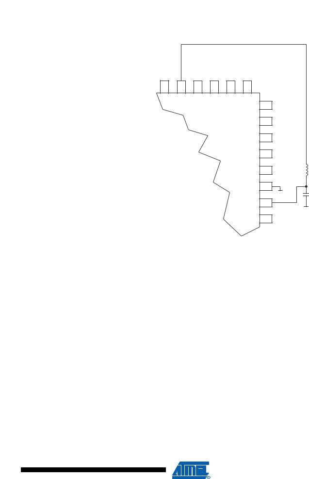
2.The AVCC pin on the device should be connected to the digital VCC supply voltage via an LC network as shown in Figure 106.
3.Use the ADC noise canceler function to reduce induced noise from the CPU.
4.If any ADC port pins are used as digital outputs, it is essential that these do not switch while a conversion is in progress.
212 ATmega16(L)
2466P–AVR–08/07
 ATmega16(L)
Figure 106. ADC Power Connections
GND |
VCC |
PA0(ADC0) |
PA1(ADC1) |
PA2(ADC2) |
PA3(ADC3) |
PA4 (ADC4)
PA5 (ADC5)
PA6 (ADC6)
PA7 (ADC7) |
|
|
AREF |
H |
|
10μ |
||
|
||
GND |
100nF |
|
AVCC |
||
|
PC7
Offset Compensation |
The gain stage has a built-in offset cancellation circuitry that nulls the offset of differential mea- |
Schemes |
surements as much as possible. The remaining offset in the analog path can be measured |
|
directly by selecting the same channel for both differential inputs. This offset residue can be then |
|
subtracted in software from the measurement results. Using this kind of software based offset |
|
correction, offset on any channel can be reduced below one LSB. |
ADC Accuracy |
An n-bit single-ended ADC converts a voltage linearly between GND and VREF in 2n steps |
Definitions |
(LSBs). The lowest code is read as 0, and the highest code is read as 2n-1. |
Several parameters describe the deviation from the ideal behavior:
•Offset: The deviation of the first transition (0x000 to 0x001) compared to the ideal transition (at 0.5 LSB). Ideal value: 0 LSB.
213
2466P–AVR–08/07

Figure 107. Offset Error
Output Code
Ideal ADC
Actual ADC
Offset
 Error
Error 
VREF Input Voltage
•Gain Error: After adjusting for offset, the Gain Error is found as the deviation of the last transition (0x3FE to 0x3FF) compared to the ideal transition (at 1.5 LSB below maximum). Ideal value: 0 LSB
Figure 108. Gain Error
Output Code |
Gain |
|
|
Error |
|
|
|
Ideal ADC |
|
|
Actual ADC |
|
VREF |
Input Voltage |
•Integral Non-linearity (INL): After adjusting for offset and gain error, the INL is the maximum deviation of an actual transition compared to an ideal transition for any code. Ideal value: 0 LSB.
214 ATmega16(L)
2466P–AVR–08/07

 ATmega16(L)
Figure 109. Integral Non-linearity (INL) |
|
Output Code |
|
INL |
Ideal ADC |
|
|
|
Actual ADC |
VREF |
Input Voltage |
•Differential Non-linearity (DNL): The maximum deviation of the actual code width (the interval between two adjacent transitions) from the ideal code width (1 LSB). Ideal value: 0 LSB.
Figure 110. Differential Non-linearity (DNL)
Output Code 
0x3FF
|
1 LSB |
|
DNL |
0x000 |
|
0 |
VREF Input Voltage |
•Quantization Error: Due to the quantization of the input voltage into a finite number of codes, a range of input voltages (1 LSB wide) will code to the same value. Always ±0.5 LSB.
•Absolute Accuracy: The maximum deviation of an actual (unadjusted) transition compared to an ideal transition for any code. This is the compound effect of Offset, Gain Error, Differential Error, Non-linearity, and Quantization Error. Ideal value: ±0.5 LSB.
215
2466P–AVR–08/07

ADC Conversion
Result
After the conversion is complete (ADIF is high), the conversion result can be found in the ADC Result Registers (ADCL, ADCH).
For single ended conversion, the result is
ADC VIN 1024
= --------------------------
VREF
where VIN is the voltage on the selected input pin and VREF the selected voltage reference (see Table 83 on page 217 and Table 84 on page 218). 0x000 represents ground, and 0x3FF represents the selected reference voltage minus one LSB.
If differential channels are used, the result is
ADC (VPOS – VNEG) GAIN 512
= -----------------------------------------------------------------------
VREF
where VPOS is the voltage on the positive input pin, VNEG the voltage on the negative input pin, GAIN the selected gain factor, and VREF the selected voltage reference. The result is presented in two’s complement form, from 0x200 (-512d) through 0x1FF (+511d). Note that if the user wants to perform a quick polarity check of the results, it is sufficient to read the MSB of the result (ADC9 in ADCH). If this bit is one, the result is negative, and if this bit is zero, the result is positive. Figure 111 shows the decoding of the differential input range.
Table 82 shows the resulting output codes if the differential input channel pair (ADCn - ADCm) is selected with a gain of GAIN and a reference voltage of VREF.
Figure 111. Differential Measurement Range
Output Code
0x1FF
0x000
- VREF/GAIN |
0x3FF |
0 |
VREF/GAIN Differential Input |
|
|
|
Voltage (Volts) |
0x200
216 ATmega16(L)
2466P–AVR–08/07

 ATmega16(L)
ADC Multiplexer
Selection Register –
ADMUX
Table 82. Correlation between Input Voltage and Output Codes
VADCn |
Read code |
Corresponding Decimal Value |
VADCm + VREF/GAIN |
0x1FF |
511 |
|
|
|
VADCm + 511/512 VREF/GAIN |
0x1FF |
511 |
VADCm + 510/512 VREF/GAIN |
0x1FE |
510 |
... |
... |
... |
|
|
|
VADCm + 1/512 VREF/GAIN |
0x001 |
1 |
VADCm |
0x000 |
0 |
VADCm - 1/512 VREF/GAIN |
0x3FF |
-1 |
|
|
|
... |
... |
... |
|
|
|
VADCm - 511/512 VREF/GAIN |
0x201 |
-511 |
VADCm - VREF/GAIN |
0x200 |
-512 |
|
|
|
Example:
ADMUX = 0xED (ADC3 - ADC2, 10x gain, 2.56V reference, left adjusted result)
Voltage on ADC3 is 300 mV, voltage on ADC2 is 500 mV.
ADCR = 512 * 10 * (300 - 500) / 2560 = -400 = 0x270
ADCL will thus read 0x00, and ADCH will read 0x9C. Writing zero to ADLAR right adjusts the result: ADCL = 0x70, ADCH = 0x02.
Bit |
7 |
6 |
5 |
4 |
3 |
2 |
1 |
0 |
|
|
REFS1 |
REFS0 |
ADLAR |
MUX4 |
MUX3 |
MUX2 |
MUX1 |
MUX0 |
ADMUX |
|
|
|
|
|
|
|
|
|
|
Read/Write |
R/W |
R/W |
R/W |
R/W |
R/W |
R/W |
R/W |
R/W |
|
Initial Value |
0 |
0 |
0 |
0 |
0 |
0 |
0 |
0 |
|
• Bit 7:6 – REFS1:0: Reference Selection Bits
These bits select the voltage reference for the ADC, as shown in Table 83. If these bits are changed during a conversion, the change will not go in effect until this conversion is complete (ADIF in ADCSRA is set). The internal voltage reference options may not be used if an external reference voltage is being applied to the AREF pin.
Table 83. Voltage Reference Selections for ADC
REFS1 |
REFS0 |
Voltage Reference Selection |
|
|
|
0 |
0 |
AREF, Internal Vref turned off |
|
|
|
0 |
1 |
AVCC with external capacitor at AREF pin |
|
|
|
1 |
0 |
Reserved |
|
|
|
1 |
1 |
Internal 2.56V Voltage Reference with external capacitor at AREF pin |
|
|
|
•Bit 5 – ADLAR: ADC Left Adjust Result
The ADLAR bit affects the presentation of the ADC conversion result in the ADC Data Register. Write one to ADLAR to left adjust the result. Otherwise, the result is right adjusted. Changing the ADLAR bit will affect the ADC Data Register immediately, regardless of any ongoing conver-
217
2466P–AVR–08/07

sions. For a complete description of this bit, see “The ADC Data Register – ADCL and ADCH” on page 220.
• Bits 4:0 – MUX4:0: Analog Channel and Gain Selection Bits
The value of these bits selects which combination of analog inputs are connected to the ADC. These bits also select the gain for the differential channels. See Table 84 for details. If these bits are changed during a conversion, the change will not go in effect until this conversion is complete (ADIF in ADCSRA is set).
Table 84. Input Channel and Gain Selections
|
Single Ended |
Positive Differential |
Negative Differential |
|
MUX4..0 |
Input |
Input |
Input |
Gain |
|
|
|
|
|
00000 |
ADC0 |
|
|
|
|
|
|
|
|
00001 |
ADC1 |
|
|
|
|
|
|
|
|
00010 |
ADC2 |
|
|
|
|
|
|
|
|
00011 |
ADC3 |
N/A |
|
|
|
|
|
|
|
00100 |
ADC4 |
|
|
|
|
|
|
|
|
00101 |
ADC5 |
|
|
|
|
|
|
|
|
00110 |
ADC6 |
|
|
|
|
|
|
|
|
00111 |
ADC7 |
|
|
|
01000 |
|
ADC0 |
ADC0 |
10x |
|
|
|
|
|
01001 |
|
ADC1 |
ADC0 |
10x |
|
|
|
|
|
01010(1) |
|
ADC0 |
ADC0 |
200x |
01011(1) |
|
ADC1 |
ADC0 |
200x |
01100 |
|
ADC2 |
ADC2 |
10x |
|
|
|
|
|
01101 |
|
ADC3 |
ADC2 |
10x |
|
|
|
|
|
01110(1) |
|
ADC2 |
ADC2 |
200x |
01111(1) |
|
ADC3 |
ADC2 |
200x |
10000 |
|
ADC0 |
ADC1 |
1x |
|
|
|
|
|
10001 |
|
ADC1 |
ADC1 |
1x |
|
|
|
|
|
10010 |
N/A |
ADC2 |
ADC1 |
1x |
|
|
|
|
|
10011 |
|
ADC3 |
ADC1 |
1x |
|
|
|
|
|
10100 |
|
ADC4 |
ADC1 |
1x |
|
|
|
|
|
10101 |
|
ADC5 |
ADC1 |
1x |
|
|
|
|
|
10110 |
|
ADC6 |
ADC1 |
1x |
|
|
|
|
|
10111 |
|
ADC7 |
ADC1 |
1x |
|
|
|
|
|
11000 |
|
ADC0 |
ADC2 |
1x |
|
|
|
|
|
11001 |
|
ADC1 |
ADC2 |
1x |
|
|
|
|
|
11010 |
|
ADC2 |
ADC2 |
1x |
|
|
|
|
|
11011 |
|
ADC3 |
ADC2 |
1x |
|
|
|
|
|
11100 |
|
ADC4 |
ADC2 |
1x |
|
|
|
|
|
218 ATmega16(L) 
2466P–AVR–08/07

 ATmega16(L)
ADC Control and
Status Register A –
ADCSRA
Table 84. |
Input Channel and Gain Selections (Continued) |
|
|
|||
|
|
Single Ended |
Positive Differential |
Negative Differential |
|
|
MUX4..0 |
|
Input |
Input |
Input |
Gain |
|
|
|
|
|
|
|
|
11101 |
|
|
ADC5 |
ADC2 |
1x |
|
|
|
|
|
|
|
|
11110 |
|
1.22 V (VBG) |
N/A |
|
|
|
11111 |
|
0 V (GND) |
|
|
|
|
|
|
|
|
|
|
|
Note: 1. |
The differential input channels are not tested for devices in PDIP Package. This feature is only |
|||||
|
guaranteed to work for devices in TQFP and QFN/MLF Packages |
|
|
|||
Bit |
7 |
6 |
5 |
4 |
3 |
2 |
1 |
0 |
|
|
ADEN |
ADSC |
ADATE |
ADIF |
ADIE |
ADPS2 |
ADPS1 |
ADPS0 |
ADCSRA |
|
|
|
|
|
|
|
|
|
|
Read/Write |
R/W |
R/W |
R/W |
R/W |
R/W |
R/W |
R/W |
R/W |
|
Initial Value |
0 |
0 |
0 |
0 |
0 |
0 |
0 |
0 |
|
• Bit 7 – ADEN: ADC Enable
Writing this bit to one enables the ADC. By writing it to zero, the ADC is turned off. Turning the ADC off while a conversion is in progress, will terminate this conversion.
• Bit 6 – ADSC: ADC Start Conversion
In Single Conversion mode, write this bit to one to start each conversion. In Free Running Mode, write this bit to one to start the first conversion. The first conversion after ADSC has been written after the ADC has been enabled, or if ADSC is written at the same time as the ADC is enabled, will take 25 ADC clock cycles instead of the normal 13. This first conversion performs initialization of the ADC.
ADSC will read as one as long as a conversion is in progress. When the conversion is complete, it returns to zero. Writing zero to this bit has no effect.
• Bit 5 – ADATE: ADC Auto Trigger Enable
When this bit is written to one, Auto Triggering of the ADC is enabled. The ADC will start a conversion on a positive edge of the selected trigger signal. The trigger source is selected by setting the ADC Trigger Select bits, ADTS in SFIOR.
• Bit 4 – ADIF: ADC Interrupt Flag
This bit is set when an ADC conversion completes and the Data Registers are updated. The ADC Conversion Complete Interrupt is executed if the ADIE bit and the I-bit in SREG are set. ADIF is cleared by hardware when executing the corresponding interrupt handling vector. Alternatively, ADIF is cleared by writing a logical one to the flag. Beware that if doing a Read-Modify- Write on ADCSRA, a pending interrupt can be disabled. This also applies if the SBI and CBI instructions are used.
• Bit 3 – ADIE: ADC Interrupt Enable
When this bit is written to one and the I-bit in SREG is set, the ADC Conversion Complete Interrupt is activated.
219
2466P–AVR–08/07

• Bits 2:0 – ADPS2:0: ADC Prescaler Select Bits
These bits determine the division factor between the XTAL frequency and the input clock to the
ADC.
Table 85. ADC Prescaler Selections
ADPS2 |
ADPS1 |
ADPS0 |
Division Factor |
|
|
|
|
0 |
0 |
0 |
2 |
|
|
|
|
0 |
0 |
1 |
2 |
|
|
|
|
0 |
1 |
0 |
4 |
|
|
|
|
0 |
1 |
1 |
8 |
|
|
|
|
1 |
0 |
0 |
16 |
|
|
|
|
1 |
0 |
1 |
32 |
|
|
|
|
1 |
1 |
0 |
64 |
|
|
|
|
1 |
1 |
1 |
128 |
|
|
|
|
The ADC Data
Register – ADCL and
ADCH
ADLAR = 0
Bit |
15 |
14 |
13 |
12 |
11 |
10 |
9 |
8 |
|
|
– |
– |
– |
– |
– |
– |
ADC9 |
ADC8 |
ADCH |
|
|
|
|
|
|
|
|
|
|
|
ADC7 |
ADC6 |
ADC5 |
ADC4 |
ADC3 |
ADC2 |
ADC1 |
ADC0 |
ADCL |
|
|
|
|
|
|
|
|
|
|
|
7 |
6 |
5 |
4 |
3 |
2 |
1 |
0 |
|
Read/Write |
R |
R |
R |
R |
R |
R |
R |
R |
|
|
R |
R |
R |
R |
R |
R |
R |
R |
|
Initial Value |
0 |
0 |
0 |
0 |
0 |
0 |
0 |
0 |
|
|
0 |
0 |
0 |
0 |
0 |
0 |
0 |
0 |
|
ADLAR = 1
Bit |
15 |
14 |
13 |
12 |
11 |
10 |
9 |
8 |
|
|
ADC9 |
ADC8 |
ADC7 |
ADC6 |
ADC5 |
ADC4 |
ADC3 |
ADC2 |
ADCH |
|
|
|
|
|
|
|
|
|
|
|
ADC1 |
ADC0 |
– |
– |
– |
– |
– |
– |
ADCL |
|
|
|
|
|
|
|
|
|
|
|
7 |
6 |
5 |
4 |
3 |
2 |
1 |
0 |
|
Read/Write |
R |
R |
R |
R |
R |
R |
R |
R |
|
|
R |
R |
R |
R |
R |
R |
R |
R |
|
Initial Value |
0 |
0 |
0 |
0 |
0 |
0 |
0 |
0 |
|
|
0 |
0 |
0 |
0 |
0 |
0 |
0 |
0 |
|
When an ADC conversion is complete, the result is found in these two registers. If differential channels are used, the result is presented in two’s complement form.
When ADCL is read, the ADC Data Register is not updated until ADCH is read. Consequently, if the result is left adjusted and no more than 8-bit precision is required, it is sufficient to read ADCH. Otherwise, ADCL must be read first, then ADCH.
The ADLAR bit in ADMUX, and the MUXn bits in ADMUX affect the way the result is read from the registers. If ADLAR is set, the result is left adjusted. If ADLAR is cleared (default), the result is right adjusted.
220 ATmega16(L)
2466P–AVR–08/07
 ATmega16(L)
Special FunctionIO
Register – SFIOR
• ADC9:0: ADC Conversion Result
These bits represent the result from the conversion, as detailed in “ADC Conversion Result” on page 216.
Bit |
7 |
6 |
5 |
4 |
3 |
2 |
1 |
0 |
|
|
ADTS2 |
ADTS1 |
ADTS0 |
– |
ACME |
PUD |
PSR2 |
PSR10 |
SFIOR |
Read/Write |
R/W |
R/W |
R/W |
R |
R/W |
R/W |
R/W |
R/W |
|
Initial Value |
0 |
0 |
0 |
0 |
0 |
0 |
0 |
0 |
|
• Bit 7:5 – ADTS2:0: ADC Auto Trigger Source
If ADATE in ADCSRA is written to one, the value of these bits selects which source will trigger an ADC conversion. If ADATE is cleared, the ADTS2:0 settings will have no effect. A conversion will be triggered by the rising edge of the selected Interrupt Flag. Note that switching from a trigger source that is cleared to a trigger source that is set, will generate a positive edge on the trigger signal. If ADEN in ADCSRA is set, this will start a conversion. Switching to Free Running mode (ADTS[2:0]=0) will not cause a trigger event, even if the ADC Interrupt Flag is set.
Table 86. ADC Auto Trigger Source Selections
ADTS2 |
ADTS1 |
ADTS0 |
Trigger Source |
|
|
|
|
0 |
0 |
0 |
Free Running mode |
|
|
|
|
0 |
0 |
1 |
Analog Comparator |
|
|
|
|
0 |
1 |
0 |
External Interrupt Request 0 |
|
|
|
|
0 |
1 |
1 |
Timer/Counter0 Compare Match |
|
|
|
|
1 |
0 |
0 |
Timer/Counter0 Overflow |
|
|
|
|
1 |
0 |
1 |
Timer/Counter1 Compare Match B |
|
|
|
|
1 |
1 |
0 |
Timer/Counter1 Overflow |
|
|
|
|
1 |
1 |
1 |
Timer/Counter1 Capture Event |
|
|
|
|
• Bit 4 – Res: Reserved Bit
This bit is reserved for future use. To ensure compatibility with future devices, this bit must be written to zero when SFIOR is written.
221
2466P–AVR–08/07