

- •Features
- •Disclaimer
- •Overview
- •Block Diagram
- •Pin Descriptions
- •Port A (PA7..PA0)
- •Port B (PB7..PB0)
- •Port C (PC7..PC0)
- •Port D (PD7..PD0)
- •RESET
- •XTAL1
- •XTAL2
- •AVCC
- •AREF
- •Resources
- •Data Retention
- •AVR CPU Core
- •Introduction
- •Status Register
- •Stack Pointer
- •I/O Memory
- •Clock Systems and their Distribution
- •Clock Sources
- •Crystal Oscillator
- •External Clock
- •Idle Mode
- •Power-down Mode
- •Power-save Mode
- •Standby Mode
- •Analog Comparator
- •Brown-out Detector
- •Watchdog Timer
- •Port Pins
- •Resetting the AVR
- •Reset Sources
- •Power-on Reset
- •External Reset
- •Watchdog Reset
- •Watchdog Timer
- •Interrupts
- •I/O Ports
- •Introduction
- •Configuring the Pin
- •Reading the Pin Value
- •Unconnected pins
- •Alternate Port Functions
- •Register Description for I/O Ports
- •8-bit Timer/Counter0 with PWM
- •Overview
- •Registers
- •Definitions
- •Counter Unit
- •Normal Mode
- •Fast PWM Mode
- •8-bit Timer/Counter Register Description
- •Timer/Counter0 and Timer/Counter1 Prescalers
- •Internal Clock Source
- •Prescaler Reset
- •External Clock Source
- •16-bit Timer/Counter1
- •Overview
- •Registers
- •Definitions
- •Compatibility
- •Counter Unit
- •Input Capture Unit
- •Noise Canceler
- •Force Output Compare
- •Normal Mode
- •Fast PWM Mode
- •16-bit Timer/Counter Register Description
- •8-bit Timer/Counter2 with PWM and Asynchronous Operation
- •Overview
- •Registers
- •Definitions
- •Counter Unit
- •Normal Mode
- •Fast PWM Mode
- •8-bit Timer/Counter Register Description
- •Slave Mode
- •Master Mode
- •Data Modes
- •USART
- •Overview
- •Clock Generation
- •External Clock
- •Frame Formats
- •Parity Bit Calculation
- •Parity Generator
- •Receiver Error Flags
- •Parity Checker
- •Disabling the Receiver
- •Using MPCM
- •Write Access
- •Read Access
- •Features
- •TWI Terminology
- •Transferring Bits
- •Address Packet Format
- •Data Packet Format
- •Overview of the TWI Module
- •SCL and SDA Pins
- •Bus Interface Unit
- •Address Match Unit
- •Control Unit
- •Using the TWI
- •Master Receiver Mode
- •Slave Receiver Mode
- •Miscellaneous States
- •Analog Comparator Multiplexed Input
- •Analog to Digital Converter
- •Features
- •Operation
- •Changing Channel or Reference Selection
- •ADC Input Channels
- •Analog Input Circuitry
- •Features
- •Overview
- •TAP Controller
- •PRIVATE0; $8
- •PRIVATE1; $9
- •PRIVATE2; $A
- •PRIVATE3; $B
- •Bibliography
- •IEEE 1149.1 (JTAG) Boundary-scan
- •Features
- •System Overview
- •Data Registers
- •Bypass Register
- •Reset Register
- •EXTEST; $0
- •IDCODE; $1
- •AVR_RESET; $C
- •BYPASS; $F
- •Scanning the ADC
- •ATmega16 Boundary-scan Order
- •Features
- •Application Section
- •Read-While-Write and no Read- While-Write Flash Sections
- •Prevent Reading the RWW Section during Self-Programming
- •Simple Assembly Code Example for a Boot Loader
- •Fuse Bits
- •Latching of Fuses
- •Signature Bytes
- •Calibration Byte
- •Page Size
- •Signal Names
- •Chip Erase
- •Reading the Flash
- •Reading the EEPROM
- •Data Polling Flash
- •Data Polling EEPROM
- •AVR_RESET ($C)
- •PROG_ENABLE ($4)
- •Data Registers
- •Reset Register
- •Programming Enable Register
- •Programming Command Register
- •Virtual Flash Page Read Register
- •Performing Chip Erase
- •Reading the Flash
- •Reading the EEPROM
- •Electrical Characteristics
- •Absolute Maximum Ratings*
- •DC Characteristics
- •External Clock Drive Waveforms
- •External Clock Drive
- •Two-wire Serial Interface Characteristics
- •ADC Characteristics
- •Idle Supply Current
- •Pin Pullup
- •Pin Driver Strength
- •Register Summary
- •Instruction Set Summary
- •Ordering Information
- •Packaging Information
- •Errata
 ATmega16(L)
Virtual Flash Page
Read Register
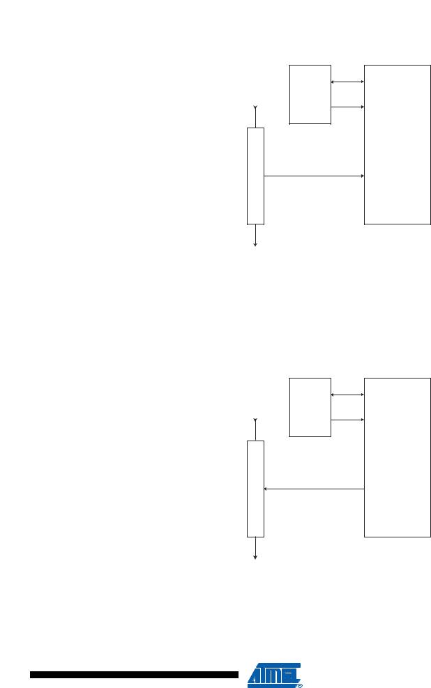
Figure 143. Virtual Flash Page Load Register
STROBES
State
Machine
TDI
ADDRESS
Flash
EEPROM
Fuses
Lock Bits
D
A
T
A
TDO
The Virtual Flash Page Read Register is a virtual scan chain with length equal to the number of bits in one Flash page plus 8. Internally the Shift Register is 8-bit, and the data are automatically transferred from the Flash data page byte by byte. The first 8 cycles are used to transfer the first byte to the internal Shift Register, and the bits that are shifted out during these 8 cycles should be ignored. Following this initialization, data are shifted out starting with the LSB of the first instruction in the page and ending with the MSB of the last instruction in the page. This provides an efficient way to read one full Flash page to verify programming.
Figure 144. Virtual Flash Page Read Register
STROBES
State
Machine
TDI
ADDRESS
Flash
EEPROM
Fuses
Lock Bits
D
A
T
A
TDO
287
2466P–AVR–08/07

Programming |
|
|
|
|
|
|
|
|
|
|
|
|
|
All references below of type “1a”, “1b”, and so on, refer to Table 117. |
||||||
Algorithm |
|
|
|
|
|
|
Entering Programming |
1. Enter JTAG instruction AVR_RESET and shift 1 in the Reset Register. |
|||||
Mode |
2. |
Enter instruction PROG_ENABLE and shift 1010_0011_0111_0000 in the Programming |
||||
|
||||||
|
|
Enable Register. |
||||
Leaving Programming |
1. Enter JTAG instruction PROG_COMMANDS. |
|||||
Mode |
2. |
Disable all programming instructions by using no operation instruction 11a. |
||||
|
||||||
|
3. |
Enter instruction PROG_ENABLE and shift 0000_0000_0000_0000 in the programming |
||||
|
|
Enable Register. |
||||
|
4. |
Enter JTAG instruction AVR_RESET and shift 0 in the Reset Register. |
||||
Performing Chip Erase |
1. Enter JTAG instruction PROG_COMMANDS. |
|||||
|
2. |
Start chip erase using programming instruction 1a. |
||||
|
3. |
Poll for Chip Erase complete using programming instruction 1b, or wait for tWLRH_CE (refer |
||||
|
|
to Table 113 on page 272). |
||||
Programming the |
Before programming the Flash a Chip Erase must be performed. See “Performing Chip Erase” |
|||||
Flash |
on page 288. |
|||||
|
1. |
Enter JTAG instruction PROG_COMMANDS. |
||||
|
2. |
Enable Flash write using programming instruction 2a. |
||||
|
3. |
Load address High byte using programming instruction 2b. |
||||
|
4. |
Load address Low byte using programming instruction 2c. |
||||
|
5. |
Load data using programming instructions 2d, 2e and 2f. |
||||
|
6. |
Repeat steps 4 and 5 for all instruction words in the page. |
||||
|
7. |
Write the page using programming instruction 2g. |
||||
|
8. |
Poll for Flash write complete using programming instruction 2h, or wait for tWLRH (refer to |
||||
|
|
Table 113 on page 272). |
||||
|
9. |
Repeat steps 3 to 7 until all data have been programmed. |
||||
A more efficient data transfer can be achieved using the PROG_PAGELOAD instruction:
1.Enter JTAG instruction PROG_COMMANDS.
2.Enable Flash write using programming instruction 2a.
3.Load the page address using programming instructions 2b and 2c. PCWORD (refer to Table 107 on page 262) is used to address within one page and must be written as 0.
4.Enter JTAG instruction PROG_PAGELOAD.
5.Load the entire page by shifting in all instruction words in the page, starting with the LSB of the first instruction in the page and ending with the MSB of the last instruction in the page.
6.Enter JTAG instruction PROG_COMMANDS.
7.Write the page using programming instruction 2g.
8.Poll for Flash write complete using programming instruction 2h, or wait for tWLRH (refer to Table 113 on page 272).
9.Repeat steps 3 to 8 until all data have been programmed.
288 ATmega16(L) 
2466P–AVR–08/07

 ATmega16(L)
Reading the Flash |
1. Enter JTAG instruction PROG_COMMANDS. |
|
|
2. |
Enable Flash read using programming instruction 3a. |
|
3. |
Load address using programming instructions 3b and 3c. |
|
4. |
Read data using programming instruction 3d. |
|
5. |
Repeat steps 3 and 4 until all data have been read. |
|
A more efficient data transfer can be achieved using the PROG_PAGEREAD instruction: |
|
|
1. |
Enter JTAG instruction PROG_COMMANDS. |
|
2. |
Enable Flash read using programming instruction 3a. |
|
3. |
Load the page address using programming instructions 3b and 3c. PCWORD (refer to |
|
|
Table 107 on page 262) is used to address within one page and must be written as 0. |
|
4. |
Enter JTAG instruction PROG_PAGEREAD. |
|
5. |
Read the entire page by shifting out all instruction words in the page, starting with the |
|
|
LSB of the first instruction in the page and ending with the MSB of the last instruction in |
|
|
the page. Remember that the first 8 bits shifted out should be ignored. |
|
6. |
Enter JTAG instruction PROG_COMMANDS. |
|
7. |
Repeat steps 3 to 6 until all data have been read. |
Programming the |
Before programming the EEPROM a Chip Erase must be performed. See “Performing Chip |
|
EEPROM |
Erase” on page 288. |
|
|
1. |
Enter JTAG instruction PROG_COMMANDS. |
|
2. |
Enable EEPROM write using programming instruction 4a. |
|
3. |
Load address High byte using programming instruction 4b. |
|
4. |
Load address Low byte using programming instruction 4c. |
|
5. |
Load data using programming instructions 4d and 4e. |
|
6. |
Repeat steps 4 and 5 for all data bytes in the page. |
|
7. |
Write the data using programming instruction 4f. |
|
8. |
Poll for EEPROM write complete using programming instruction 4g, or wait for tWLRH |
|
|
(refer to Table 113 on page 272). |
|
9. |
Repeat steps 3 to 8 until all data have been programmed. |
Note that the PROG_PAGELOAD instruction can not be used when programming the EEPROM
Reading the EEPROM 1. Enter JTAG instruction PROG_COMMANDS.
2.Enable EEPROM read using programming instruction 5a.
3.Load address using programming instructions 5b and 5c.
4.Read data using programming instruction 5d.
5.Repeat steps 3 and 4 until all data have been read.
Note that the PROG_PAGEREAD instruction can not be used when reading the EEPROM
289
2466P–AVR–08/07

Programming the |
|
|
|
|
|
|
|
|
|
|
|
|
|
1. Enter JTAG instruction PROG_COMMANDS. |
||||||
Fuses |
2. |
Enable Fuse write using programming instruction 6a. |
||||
|
||||||
|
3. |
Load data High byte using programming instructions 6b. A bit value of “0” will program |
||||
|
|
the corresponding fuse, a “1” will unprogram the fuse. |
||||
|
4. |
Write Fuse High byte using programming instruction 6c. |
||||
|
5. |
Poll for Fuse write complete using programming instruction 6d, or wait for tWLRH (refer to |
||||
|
|
Table 113 on page 272). |
||||
|
6. |
Load data Low byte using programming instructions 6e. A “0” will program the fuse, a “1” |
||||
|
|
will unprogram the fuse. |
||||
|
7. |
Write Fuse Low byte using programming instruction 6f. |
||||
|
8. |
Poll for Fuse write complete using programming instruction 6g, or wait for tWLRH (refer to |
||||
|
|
Table 113 on page 272). |
||||
Programming the Lock 1. Enter JTAG instruction PROG_COMMANDS. |
||||||
Bits |
2. |
Enable Lock bit write using programming instruction 7a. |
||||
|
||||||
|
3. |
Load data using programming instructions 7b. A bit value of “0” will program the corre- |
||||
|
|
sponding Lock bit, a “1” will leave the Lock bit unchanged. |
||||
|
4. |
Write Lock bits using programming instruction 7c. |
||||
|
5. |
Poll for Lock bit write complete using programming instruction 7d, or wait for tWLRH (refer |
||||
|
|
to Table 113 on page 272). |
||||
Reading the Fuses |
1. Enter JTAG instruction PROG_COMMANDS. |
|||||
and Lock Bits |
2. |
Enable Fuse/Lock bit read using programming instruction 8a. |
||||
|
||||||
|
3. |
To read all Fuses and Lock bits, use programming instruction 8e. |
||||
|
|
To only read Fuse High byte, use programming instruction 8b. |
||||
|
|
To only read Fuse Low byte, use programming instruction 8c. |
||||
|
|
To only read Lock bits, use programming instruction 8d. |
||||
Reading the Signature 1. Enter JTAG instruction PROG_COMMANDS. |
||||||
Bytes |
2. |
Enable Signature byte read using programming instruction 9a. |
||||
|
||||||
|
3. |
Load address $00 using programming instruction 9b. |
||||
|
4. |
Read first signature byte using programming instruction 9c. |
||||
|
5. |
Repeat steps 3 and 4 with address $01 and address $02 to read the second and third |
||||
|
|
signature bytes, respectively. |
||||
Reading the |
1. |
Enter JTAG instruction PROG_COMMANDS. |
||||
Calibration Byte |
2. |
Enable Calibration byte read using programming instruction 10a. |
||||
|
||||||
|
3. |
Load address $00 using programming instruction 10b. |
||||
|
4. |
Read the calibration byte using programming instruction 10c. |
||||
290 ATmega16(L) 
2466P–AVR–08/07