


 ATmega128(L)
8-bit Timer/Counter0 with PWM and Asynchronous Operation
Timer/Counter0 is a general purpose, single channel, 8-bit Timer/Counter module. The main features are:
•Single Channel Counter
•Clear Timer on Compare Match (Auto Reload)
•Glitch-free, Phase Correct Pulse Width Modulator (PWM)
•Frequency Generator
•10-bit Clock Prescaler
•Overflow and Compare Match Interrupt Sources (TOV0 and OCF0)
•Allows Clocking from External 32 kHz Watch Crystal Independent of the I/O Clock
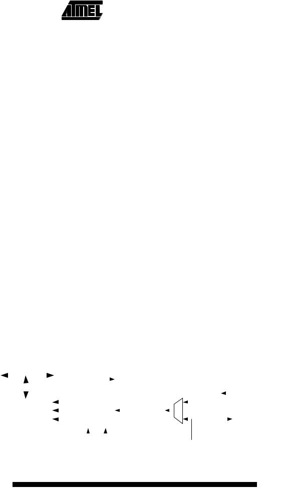
Overview |
A simplified block diagram of the 8-bit Timer/Counter is shown in Figure 33. For the |
|||||||||||||||||||||||||||||||||||||||||||
|
actual placement of I/O pins, refer to “Pin Configurations” on page 2. CPU accessible |
|||||||||||||||||||||||||||||||||||||||||||
|
I/O registers, including I/O bits and I/O pins, are shown in bold. The device-specific I/O |
|||||||||||||||||||||||||||||||||||||||||||
|
register and bit locations are listed in the “8-bit Timer/Counter Register Description” on |
|||||||||||||||||||||||||||||||||||||||||||
|
page 98. |
|
|
|
|
|
|
|
|
|
|
|
|
|
|
|
|
|
|
|
|
|
|
|
|
|
|
|
|
|||||||||||||||
|
Figure 33. 8-bit Timer/Counter Block Diagram |
|
|
|
|
|
|
|
|
|
|
|
||||||||||||||||||||||||||||||||
|
|
|
|
|
|
|
|
|
|
|
|
|
|
|
|
|
|
|
|
|
|
|
|
|
|
|
|
|
|
|
|
|
|
|
|
|
|
|
|
|
|
|
|
|
|
|
|
|
|
|
|
|
|
|
|
|
|
|
|
|
|
|
TCCRn |
|
|
|
|
|
|
|
|
|
|
|
|
|
|
|
|
|
|
|
|
||||||
|
|
|
|
|
|
|
|
|
|
|
count |
|
|
|
|
|
|
|
|
TOVn |
||||||||||||||||||||||||
|
|
|
|
|
|
|
|
|
|
|
|
|
|
|
|
|
|
|
|
|
|
|
|
|
|
|
|
|
|
|
|
|
|
|
|
|||||||||
|
|
|
|
|
|
|
|
|
|
|
|
|
|
|
|
|
|
|
|
|
|
|
|
|
|
|
|
|
|
|
|
|
|
|
|
|||||||||
|
|
|
|
|
|
|
|
|
|
|
|
|
|
|
|
|
|
|
|
|
|
|
|
|
|
|
|
|
|
|
|
|
|
|
|
|||||||||
|
|
|
|
|
|
|
|
|
|
|
|
|
|
|
|
|
|
|
|
|
|
|
|
|
|
|
|
|
|
|
|
|
|
|
|
|||||||||
|
|
|
|
|
|
|
|
|
|
|
|
|
|
|
|
|
|
|
|
|
|
|
|
|
|
|
|
|
|
|
|
|
|
|
|
|
|
|
|
|||||
|
|
|
|
|
|
|
|
|
|
|
clear |
|
|
Control Logic |
|
|
|
|
|
|
|
|
|
|
|
|
|
|
|
|
|
(Int.Req.) |
||||||||||||
|
|
|
|
|
|
|
|
|
|
|
|
|
|
|
|
|
|
|
|
|
|
|
|
|
|
|
|
|
|
|
|
|
|
|
||||||||||
|
|
|
|
|
|
|
|
|
|
|
|
|
|
|
|
|
clkTn |
|
|
|
|
|
|
|
|
|
|
|
||||||||||||||||
|
|
|
|
|
|
|
|
|
|
|
direction |
|
|
|
|
|
|
|
|
|
|
|
|
|
|
|
|
|
|
|
||||||||||||||
|
|
|
|
|
|
|
|
|
|
|
|
|
|
|
|
|
|
|
|
|
|
|
|
|
|
|
|
|
|
|
|
|
|
|
|
|
|
|
|
|
|
|
TOSC1 |
|
|
|
|
|
|
|
|
|
|
|
|
|
|
|
|
|
|
|
|
|
|
|
|
|
|
|
|
|
|
|
|
|
|
|
|
|
|
|
|
|
|
|
|
|
|
|
|
|
|
|
|
|
|
|
|
|
|
|
|
|
|
|
|
|
|
|
|
|
|
|
|
|
|
|
|
|
|
|
|
|
|
|
|
|||||||
|
|
|
|
|
|
|
|
|
|
|
|
BOTTOM |
|
|
TOP |
|
|
|
|
|
|
|
|
|
T/C |
|
|
|
|
|
||||||||||||||
|
|
|
|
|
|
|
|
|
|
|
|
|
|
|
|
|
|
|
|
|
|
|||||||||||||||||||||||
|
|
|
|
|
|
|
|
|
|
|
|
|
|
|
|
|
|
|
|
|
|
|
|
|
|
|
|
|
|
|
|
|
|
|
|
|
|
|
|
|||||
|
|
|
|
|
|
|
|
|
|
|
|
|
|
|
|
|
|
|
|
|
|
|
|
|
|
|
|
Prescaler |
|
|
|
|
|
|
|
Oscillator |
|
|
|
|||||
|
|
|
|
|
|
|
|
|
|
|
|
|
|
|
|
|
|
|
|
|
|
|
|
|
|
|
|
|
|
|
|
|
|
|
|
|
|
|
|
|
|
|
TOSC2 |
|
|
|
|
|
|
|
|
|
|
|
|
|
|
|
|
|
|
|
|
|
|
|
|
|
|
|
|
|
|
|
|
|
|
|
|
|
|
|
|
|
|
|
|
|
|
|
|
|
|
|
|
Timer/Counter |
|
|
|
|
|
|
|
|
|
|
|
|
|
|
|
|
|
|
|
|
|
|
|
|
|
|
|
|
|
|
|
|
||||||
|
|
|
|
|
|
|
|
TCNTn |
|
|
|
|
|
|
|
|
|
|
|
|
|
|
|
|
|
|
|
|
|
|
|
|
|
|
|
|
|
|
|
|
|
|||
|
|
|
|
|
|
|
|
|
|
|
|
|
|
= 0 |
|
= 0xFF |
|
|
|
|
|
|
|
|
|
|
|
|
|
|
|
|
clk I/O |
|||||||||||
|
|
|
|
|
|
|
|
|
|
|
|
|
|
|
|
|
|
|
||||||||||||||||||||||||||
|
|
|
|
|
|
|
|
|
|
|
|
|
|
|
|
|
|
|
|
|
|
|
|
|
|
|
OCn |
|
|
|
|
|
|
|||||||||||
|
|
|
|
|
|
|
|
|
|
|
|
|
|
|
|
|
|
|
|
|
|
|
|
|
|
|
|
|
|
|
|
|
||||||||||||
|
|
|
|
|
|
|
|
|
|
|
|
|
|
|
|
|
|
|
|
|
|
|
|
|
|
|
(Int.Req.) |
|
|
|
|
|
|
|
|
|
|
|
||||||
|
|
|
|
|
|
|
|
|
|
|
|
|
|
|
|
|
|
|
|
|
|
|
|
|
|
|
|
|
|
|
|
|
|
|
|
|
|
|
|
|
|
|
|
|
|
|
|
|
|
|
|
|
|
|
|
|
|
|
|
|
|
|
|
|
|
|
|
|
|
|
|
|
Waveform |
|
|
|
|
|
|
|
|
|
|
|
|
|
|
||
|
|
|
|
|
|
|
= |
|
|
|
|
|
|
|
|
|
|
|
|
|
OCn |
|
|
|
||||||||||||||||||||
|
|
|
|
|
|
|
|
|
|
|
|
|
|
|
|
|
|
|
|
|
|
|
|
|
Generation |
|
|
|
|
|
|
|
|
|
|
|
|
|||||||
|
|
|
|
|
|
|
|
|
|
|
|
|
|
|
|
|
|
|
|
|
|
|
|
|
|
|
|
|
|
|
|
|
|
|
|
|
|
|
|
|
|
|||
|
|
|
|
|
|
|
|
|
|
|
|
|
|
|
|
|
|
|
|
|
|
|
|
|
|
|
|
|
|
|
|
|
|
|
|
|
|
|
|
|
|
|
|
|
|
|
|
|
|
|
|
|
|
|
|
|
|
|
|
|
|
|
|
|
|
|
|
|
|
|
|
|
|
|
|
|
|
|
|
|
|
|
|
|
|
|
|||
|
DATABUS |
|
|
|
|
|
|
OCRn |
|
|
|
|
|
|
|
|
|
|
|
|
|
|
|
|
|
|
|
|
|
|
|
|
|
|
|
|
|
|
||||||
|
|
|
|
|
|
|
|
|
|
|
|
|
|
|
|
|
|
|
|
|
|
|
|
|
|
|
|
|
|
|
|
|
|
|
|
|
|
|
|
|||||
|
|
|
|
|
|
|
|
|
|
|
|
|
|
|
|
|
|
|
|
|
|
|
|
|
|
|
|
|
|
|
|
|
|
|
|
|
|
|
|
|
|
|||
|
|
|
|
|
|
|
|
|
|
|
|
|
|
|
|
|
|
|
|
|
|
|
|
|
|
|
|
|
|
|
|
|
|
|
|
|
|
|
|
|
|
|
|
|
|
|
|
|
|
|
|
|
|
|
|
|
|
|
Synchronized Status flags |
|
|
|
|
|
|
|
|
|
|
|
|
|
|
|
|
|
clk I/O |
||||||||||||
|
|
|
|
|
|
|
|
|
|
|
|
|
|
|
|
|
|
|
|
|
|
|
|
|
|
|
|
|
|
|
||||||||||||||
|
|
|
|
|
|
|
|
|
|
|
|
|
|
|
|
|
|
|
|
|
|
|
|
|
|
|
|
|
|
|
||||||||||||||
|
|
|
|
|
|
|
|
|
|
|
|
|
|
|
|
|
|
|
|
|
|
|
|
|
|
|
|
|
|
|
|
|
|
|||||||||||
|
|
|
|
|
Status flags |
|
|
|
|
|
|
|
|
|
|
|
|
|
|
|
|
Synchronization Unit |
|
|
|
|
|
|
clk ASY |
|||||||||||||||
|
|
|
|
|
|
|
|
|
|
|
|
|
|
|
|
|
|
|
|
|
|
|
|
|
|
|
|
|
|
|
|
|
|
|
|
|||||||||
|
|
|
|
|
|
|
|
|
|
|
|
|
|
|
|
|
|
|
|
|
|
|
|
|
|
|
|
|
|
|
|
|
|
|
|
|||||||||
|
|
|
|
|
|
|
|
|
|
|
|
|
|
|
|
|
|
|
|
|
|
|
|
|
|
|
|
|
|
|
|
|
|
|
|
|||||||||
|
|
|
|
|
|
|
|
|
|
|
|
|
|
|
|
|
|
|
|
|
|
|
|
|
|
|
|
|
|
|
|
|
|
|
|
|||||||||
|
|
|
|
|
|
|
|
|
|
|
ASSRn |
|
asynchronous mode |
|
|
|
|
|
|
|
|
|
|
|
|
|
|
|
|
|
||||||||||||||
|
|
|
|
|
|
|
|
|
|
|
|
|
|
|
|
|
|
|
|
|
|
|
|
|
|
|
|
|
|
|
|
|
||||||||||||
|
|
|
|
|
|
|
|
|
|
|
|
|
|
|
|
|
|
|
select (ASn) |
|
|
|
|
|
|
|
|
|
|
|
|
|
|
|
||||||||||
|
|
|
|
|
|
|
|
|
|
|
|
|
|
|
|
|
|
|
|
|
|
|
|
|
|
|
|
|
|
|
|
|
|
|
|
|
|
|
|
|
|
|
|
|
|
|
|
|
|
|
|
|
|
|
|
|
|
|
|
|
|
|
|
|
|
|
|
|
|
|
|
|
|
|
|
|
|
|
|
|
|
|
|
|
|
|
|
|
|
|
|
|
|
|
|
|
|
|
|
|
|
|
|
|
|
|
|
|
|
|
|
|
|
|
|
|
|
|
|
|
|
|
|
|
|
|
|
|
|
|
|
|
|
|
Registers |
The Timer/Counter (TCNT0) and Output Compare Register (OCR0) are 8-bit registers. |
|
Interrupt request (shorten as Int.Req.) signals are all visible in the Timer Interrupt Flag |
|
Register (TIFR). All interrupts are individually masked with the Timer Interrupt Mask reg- |
|
ister (TIMSK). TIFR and TIMSK are not shown in the figure since these registers are |
|
shared by other timer units. |
87
2467B–09/01
|
|
|
|
|
|
|
|
|
|
|
|
|
|
|
|
|
|
|
|
|
|
|
|
|
|
|
|
|
The Timer/Counter can be clocked internally, via the prescaler, or asynchronously |
|||||
|
clocked from the TOSC1/2 pins, as detailed later in this chapter. The asynchronous |
|||||
|
operation is controlled by the Asynchronous Status Register (ASSR). The Clock Select |
|||||
|
logic block controls which clock source the Timer/Counter uses to increment (or decre- |
|||||
|
ment) its value. The Timer/Counter is inactive when no clock source is selected. The |
|||||
|
output from the clock select logic is referred to as the timer clock (clkT0). |
|||||
|
The double buffered Output Compare Register (OCR0) is compared with the |
|||||
|
Timer/Counter value at all times. The result of the compare can be used by the wave- |
|||||
|
form generator to generate a PWM or variable frequency output on the Output Compare |
|||||
|
Pin (OC0). See “Output Compare Unit” on page 89. for details. The compare match |
|||||
|
event will also set the compare flag (OCF0) which can be used to generate an output |
|||||
|
compare interrupt request. |
|||||
Definitions |
Many register and bit references in this document are written in general form. A lower |
|||||
|
case “n” replaces the Timer/Counter number, in this case 0. However, when using the |
|||||
|
register or bit defines in a program, the precise form must be used (i.e., TCNT0 for |
|||||
|
accessing Timer/Counter0 counter value and so on). |
|||||
|
The definitions in Table 51 are also used extensively throughout the document. |
|||||
|
Table 51. Definitions |
|||||
|
|
|
||||
|
BOTTOM |
The counter reaches the BOTTOM when it becomes zero (0x00) |
||||
|
MAX |
The counter reaches its MAXimum when it becomes 0xFF (decimal 255). |
||||
|
TOP |
The counter reaches the TOP when it becomes equal to the highest |
||||
|
|
value in the count sequence. The TOP value can be assigned to be the |
||||
|
|
fixed value 0xFF (MAX) or the value stored in the OCR0 register. The |
||||
|
|
assignment is dependent on the mode of operation. |
||||
|
|
|
|
|
|
|
Timer/Counter Clock
Sources
Counter Unit
The Timer/Counter can be clocked by an internal synchronous or an external asynchro-
nous clock source. The clock source clkT0 is by default equal to the MCU clock, clkI/O. When the AS0 bit in the ASSR register is written to logic one, the clock source is taken
from the Timer/Counter Oscillator connected to TOSC1 and TOSC2. For details on asynchronous operation, see “Asynchronous Status Register – ASSR” on page 101. For details on clock sources and prescaler, see “Timer/Counter Prescaler” on page 104.
The main part of the 8-bit Timer/Counter is the programmable bidirectional counter unit. Figure 34 shows a block diagram of the counter and its surrounding environment.
Figure 34. Counter Unit Block Diagram
DATA BUS
|
|
|
|
|
|
|
TOVn |
|
|
|
|
|
|
|
|
|
|
|
|
|
|
|
|
|
|
|
(Int.Req.) |
|
|
|
|
|
|
|
|
|
|
|
|
|
|
|
count |
|
|
|
|
clk Tn |
|
|
|
|
|
|
T/C |
|
|
|
TOSC1 |
|
|
|
|
|
|
|
|
|
|
|
|
|
|||||||
|
|
|
|
|
|
|
|
|
|
|
|
|
|
|
|
|
|||
|
|
|
clear |
|
|
|
|
|
|
|
|
|
|
|
|
|
|||
TCNTn |
|
Control Logic |
|
Prescaler |
|
|
|
|
|
Oscillator |
|
|
|
|
|||||
|
|
|
direction |
|
|
|
|
|
|
|
|
|
|
|
|
|
|
|
TOSC2 |
|
|
|
|
|
|
|
|
|
|
|
|
|
|
|
|
|
|
|
|
|
|
|
|
|
|
|
|
|
|
|
|
|
|
|
|
|
|
|
|
|
|
|
|
|
|
|
|
|
|
|
|
|
|
|
|
|
|
|
|
bottom |
|
top |
|
clkI/O |
|
|
|||
|
|
|
|
|
88 ATmega128(L)
2467B–09/01