

 ATmega128(L)
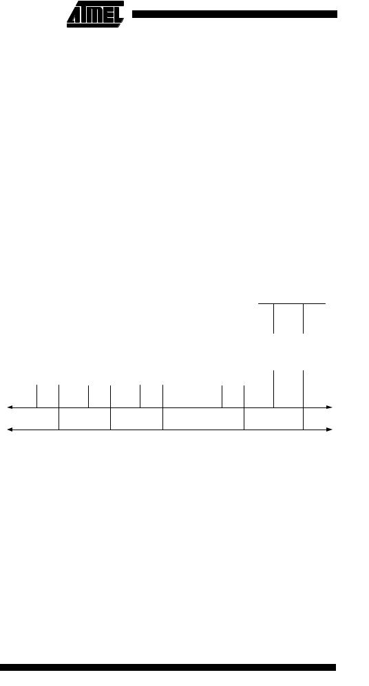
Address Packet Format |
|
|
|
|
|
|
|
|
|
|
|
|
|
|
|
|
|
|
|
|
|
|
|
|
|
|
|
|
|
|
|
|
|
|
|
|
|
|
|
|
|
|
|
|
|
|
|
|
|
|
|
All address packets transmitted on the TWI bus are 9 bits long, consisting of 7 address |
||||||||||||
|
bits, one READ/WRITE control bit and an acknowledge bit. If the READ/WRITE bit is |
|||||||||||
|
set, a read operation is to be performed, otherwise a write operation should be per- |
|||||||||||
|
formed. When a slave recognizes that it is being addressed, it should acknowledge by |
|||||||||||
|
pulling SDA low in the ninth SCL (ACK) cycle. If the addressed slave is busy, or for |
|||||||||||
|
some other reason can not service the master’s request, the SDA line should be left |
|||||||||||
|
high in the ACK clock cycle. The master can then transmit a STOP condition, or a |
|||||||||||
|
REPEATED START condition to initiate a new transmission. An address packet consist- |
|||||||||||
|
ing of a slave address and a READ or a WRITE bit is called SLA+R or SLA+W, |
|||||||||||
|
respectively. |
|
|
|
|
|
|
|
|
|||
|
The MSB of the address byte is transmitted first. Slave addresses can freely be allo- |
|||||||||||
|
cated by the designer, but the address 0000 000 is reserved for a general call. |
|||||||||||
|
When a general call is issued, all slaves should respond by pulling the SDA line low in |
|||||||||||
|
the ACK cycle. A general call is used when a master wishes to transmit the same mes- |
|||||||||||
|
sage to several slaves in the system. When the general call address followed by a Write |
|||||||||||
|
bit is transmitted on the bus, all slaves set up to acknowledge the general call will pull |
|||||||||||
|
the SDA line low in the ack cycle. The following data packets will then be received by all |
|||||||||||
|
the slaves that acknowledged the general call. Note that transmitting the general call |
|||||||||||
|
address followed by a Read bit is meaningless, as this would cause contention if several |
|||||||||||
|
slaves started transmitting different data. |
|
|
|
|
|
||||||
|
All addresses of the format 1111 xxx should be reserved for future purposes. |
|||||||||||
|
Figure 88. Address Packet Format |
|
|
|
|
|
|
|
|
|||
|
Addr MSB |
|
|
|
|
|
Addr LSB |
R/W |
ACK |
|||
|
SDA |
|
|
|
|
|
|
|
|
|||
|
|
|
|
|
|
|
|
|
||||
|
SCL |
|
|
|
|
|
|
|
|
|||
|
|
|
|
|
|
|
|
|
||||
|
1 |
|
|
|
2 |
|
|
|
7 |
8 |
9 |
|
|
|
|
|
|
|
|||||||
|
START |
|
|
|
|
|
|
|
|
|||
Data Packet Format |
All data packets transmitted on the TWI bus are 9 bits long, consisting of one data byte |
|||||||||||
|
and an acknowledge bit. During a data transfer, the master generates the clock and the |
|||||||||||
|
START and STOP conditions, while the receiver is responsible for acknowledging the |
|||||||||||
|
reception. An Acknowledge (ACK) is signalled by the receiver pulling the SDA line low |
|||||||||||
|
during the ninth SCL cycle. If the receiver leaves the SDA line high, a NACK is signalled. |
|||||||||||
|
When the receiver has received the last byte, or for some reason cannot receive any |
|||||||||||
|
more bytes, it should inform the transmitter by sending a NACK after the final byte. The |
|||||||||||
|
MSB of the data byte is transmitted first. |
|
|
|
|
|
||||||
192 ATmega128(L)
2467B–09/01