- •Features
- •Pin Configuration
- •Description
- •Block Diagram
- •Pin Descriptions
- •AVCC
- •Port A (PA7..PA0)
- •Port B (PB7..PB0)
- •XTAL1
- •XTAL2
- •Resources
- •AVR CPU Core
- •Architectural Overview
- •I/O Direct
- •Data Direct
- •Data Indirect with Displacement
- •Data Indirect
- •Memories
- •SRAM Data Memory
- •EEPROM Data Memory
- •EEPROM Read/Write Access
- •I/O Memory
- •Clock Systems and their Distribution
- •Clock Sources
- •Default Clock Source
- •Crystal Oscillator
- •External RC Oscillator
- •External Clock
- •Power-on Reset
- •External Reset
- •Brown-out Detection
- •Watchdog Reset
- •Idle Mode
- •Power-down Mode
- •Standby Mode
- •Analog to Digital Converter
- •Analog Comparator
- •Brown-out Detector
- •Internal Voltage Reference
- •Watchdog Timer
- •Port Pins
- •I/O Ports
- •Introduction
- •Configuring the Pin
- •Reading the Pin Value
- •Unconnected Pins
- •Alternate Port Functions
- •Alternate Functions of Port A
- •Alternate Functions Of Port B
- •Register Description for I/O Ports
- •Interrupts
- •Interrupt Vectors
- •Interrupt Handling
- •Interrupt Response Time
- •External Interrupt
- •Pin Change Interrupt
- •Timer/Counters
- •Timer/Counter0 Prescaler
- •Timer/Counter1 Prescaler
- •8-bit Timer/Counter0
- •8-bit Timer/Counter1
- •Timer/Counter1 in PWM Mode
- •Watchdog Timer
- •Overview
- •Register Descriptions
- •Functional Descriptions
- •Three-wire Mode
- •SPI Slave Operation Example
- •Two-wire Mode
- •Start Condition Detector
- •Alternative USI Usage
- •4-bit Counter
- •12-bit Timer/Counter
- •Software Interrupt
- •Analog Comparator
- •Analog to Digital Converter
- •Features
- •Operation
- •Changing Channel or Reference Selection
- •ADC Conversion Result
- •ADLAR = 0
- •ADLAR = 1
- •Fuse Bits
- •Latching of Fuses
- •Signature Bytes
- •Calibration Byte
- •Page Size
- •Signal Names
- •Parallel Programming
- •Enter Programming Mode
- •Chip Erase
- •Programming the Flash
- •Programming the EEPROM
- •Reading the Flash
- •Reading the EEPROM
- •Programming the Lock Bits
- •Reading the Signature Bytes
- •Reading the Calibration Byte
- •Serial Downloading
- •Data Polling Flash
- •Data Polling EEPROM
- •Electrical Characteristics
- •Absolute Maximum Ratings*
- •DC Characteristics
- •External Clock Drive Waveforms
- •External Clock Drive
- •ADC Characteristics
- •Active Supply Current
- •Idle Supply Current
- •Power-down Supply Current
- •Standby Supply Current
- •Pin Pull-up
- •Internal Oscillator Speed
- •Register Summary
- •Instruction Set Summary
- •Ordering Information
- •Packaging Information
- •Errata
- •ATtiny26 Rev. B/C/D
- •Table of Contents
ATtiny26(L)
Memories
The AVR CPU is driven by the System Clock Ø, directly generated from the external clock crystal for the chip. No internal clock division is used.
Figure 16 shows the parallel instruction fetches and instruction executions enabled by the Harvard architecture and the fast-access Register File concept. This is the basic pipelining concept to obtain up to 1 MIPS per MHz with the corresponding unique results for functions per cost, functions per clocks, and functions per power-unit.
Figure 16. The Parallel Instruction Fetches and Instruction Executions
T1 |
T2 |
T3 |
T4 |
System Clock Ø
1st Instruction Fetch
1st Instruction Execute 2nd Instruction Fetch 2nd Instruction Execute 3rd Instruction Fetch 3rd Instruction Execute 4th Instruction Fetch
Figure 17 shows the internal timing concept for the Register File. In a single clock cycle an ALU operation using two register operands is executed, and the result is stored back to the destination register.
Figure 17. Single Cycle ALU Operation
T1 |
T2 |
T3 |
T4 |
System Clock Ø
Total Execution Time
Register Operands Fetch
ALU Operation Execute
Result Write Back
The internal data SRAM access is performed in two System Clock cycles as described in Figure 18.
17
1477J–AVR–06/07
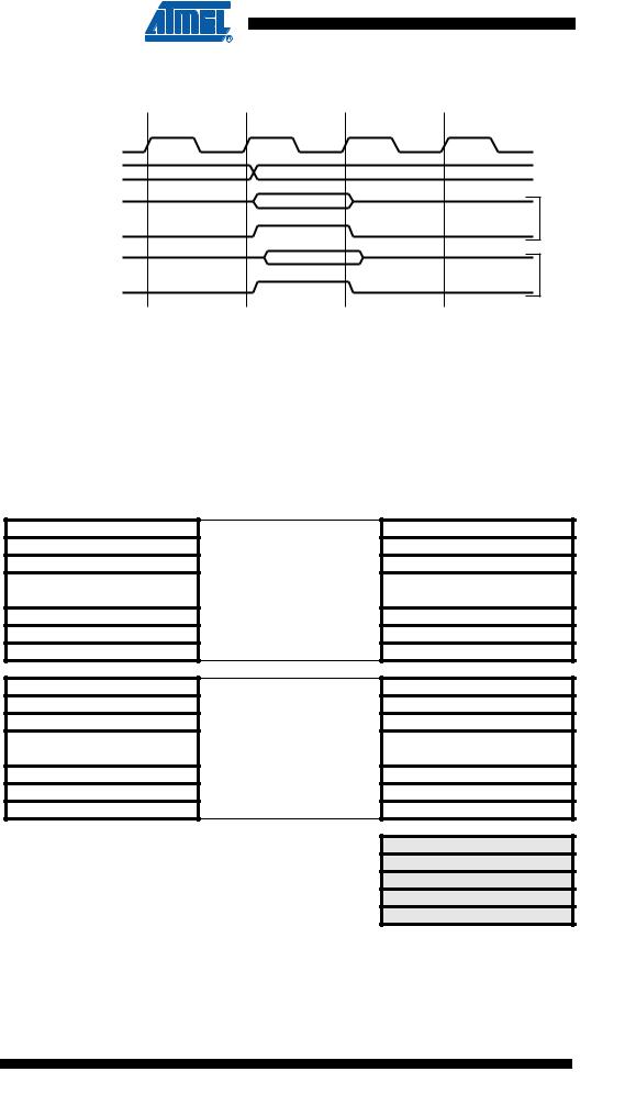
Figure 18. On-chip Data SRAM Access Cycles
T1 |
T2 |
T3 |
T4 |
System Clock Ø
Address |
Prev. Address |
Address |
Data
WR
Data
RD
Read Write
In-System Programmable
Flash Program Memory
The ATtiny26(L) contains 2K bytes On-chip In-System Programmable Flash memory for program storage. Since all instructions are 16or 32-bit words, the Flash is organized as 1K x 16. The Flash memory has an endurance of at least 10,000 write/erase cycles. The ATtiny26(L) Program Counter – PC – is 10 bits wide, thus addressing the 1024 program memory addresses, see “Memory Programming” on page 109 for a detailed description on Flash data downloading. See “Program and Data Addressing Modes” on page 12 for the different program memory addressing modes.
Figure 19. SRAM Organization
Register File
R0
R1
R2
...
R29
R30
R31
I/O Registers
$00
$01
$02
…
$3D
$3E
$3F
Data Address Space
$0000
$0001
$0002
...
$001D
$001E
$001F
$0020
$0021
$0022
…
$005D
$005E
$005F
Internal SRAM
$0060
$0061
...
$00DE
$00DF
SRAM Data Memory
Figure 19 above shows how the ATtiny26(L) SRAM Memory is organized.
The lower 224 Data Memory locations address the Register File, the I/O Memory and the internal data SRAM. The first 96 locations address the Register File and I/O Memory, and the next 128 locations address the internal data SRAM.
18 ATtiny26(L)
1477J–AVR–06/07