


Figure 96. Standby Supply Current vs. VCC (6 MHz XTAL, Watchdog Timer Disabled)
(uA)
STANDBY SUPPLY CURRENT vs. VCC
6 MHz XTAL, WATCHDOG TIMER DISABLED
180
160
140
120
100
ICC
80
60
40
20
0
2 |
2.5 |
3 |
3.5 |
4 |
4.5 |
5 |
5.5 |
VCC (V)
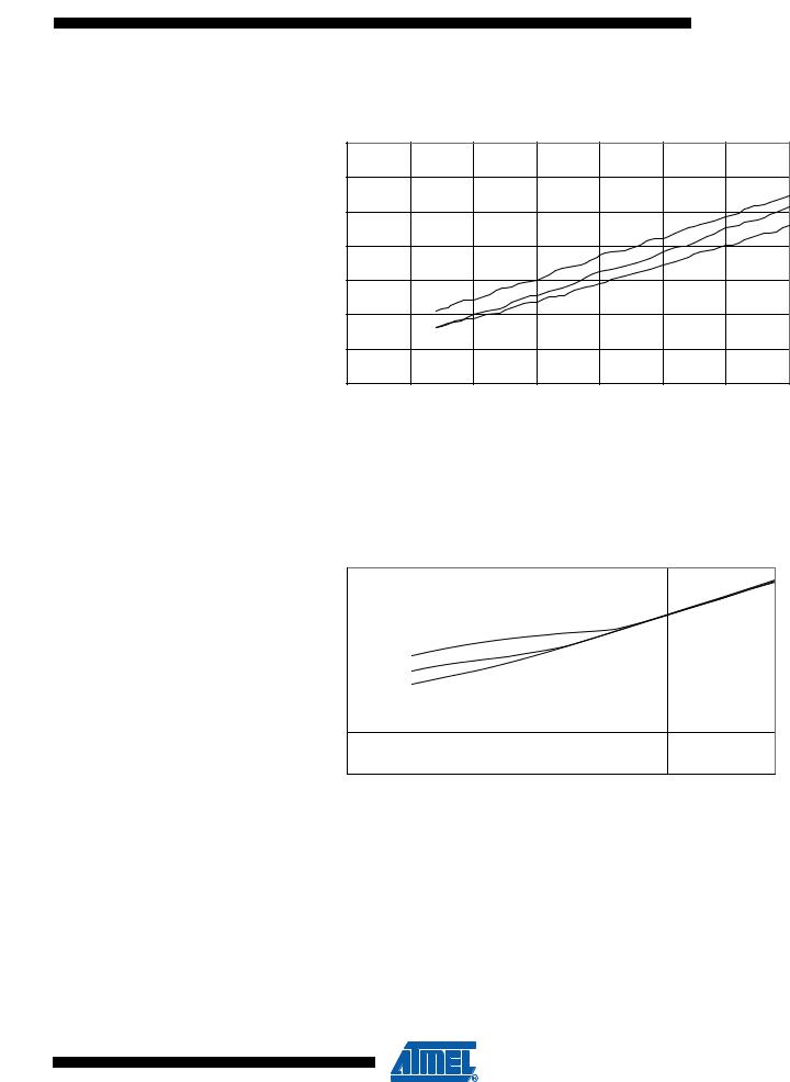
Pin Pull-up |
Figure 97. |
I/O Pin Pull-up Resistor Current vs. Input Voltage (VCC = 5V) |
|
|
||||||||
|
|
|
|
I/O PIN PULL-UP RESISTOR CURRENT vs. INPUT VOLTAGE |
|
|
||||||
|
|
|
|
|
|
Vcc = 5V |
|
|
|
|
|
|
|
|
160 |
|
|
|
|
|
|
|
|
|
|
|
85°C |
|
|
|
|
|
|
|
|
|
|
|
|
|
140 |
|
|
|
|
|
|
|
|
|
|
|
|
|
25°C |
|
|
|
|
|
|
|
|
|
|
|
|
|
|
|
|
|
|
|
|
|
|
|
|
120 |
|
|
|
|
|
|
|
|
|
|
|
|
-40°C |
|
|
|
|
|
|
|
|
||
|
|
|
|
|
|
|
|
|
|
|
||
|
(uA) |
100 |
|
|
|
|
|
|
|
|
|
|
|
|
|
|
|
|
|
|
|
|
|
||
|
80 |
|
|
|
|
|
|
|
|
|
|
|
|
|
|
|
|
|
|
|
|
|
|
||
|
OP |
|
|
|
|
|
|
|
|
|
|
|
|
|
|
|
|
|
|
|
|
|
|
|
|
|
I |
|
|
|
|
|
|
|
|
|
|
|
|
|
60 |
|
|
|
|
|
|
|
|
|
|
|
|
|
|
|
|
|
|
|
|
|
|
|
|
|
40 |
|
|
|
|
|
|
|
|
|
|
|
|
|
|
|
|
|
|
|
|
|
|
|
|
|
20 |
|
|
|
|
|
|
|
|
|
|
|
|
|
|
|
|
|
|
|
|
|
|
|
|
|
0 |
|
|
|
|
|
|
|
|
|
|
|
|
|
|
|
|
|
|
|
|
|
|
|
|
|
0 |
1 |
2 |
3 |
4 |
5 |
6 |
||||
|
|
|
|
|
|
VOP (V) |
|
|
|
|
|
|
146 ATtiny26(L)
1477J–AVR–06/07

 ATtiny26(L)
Figure 98. I/O Pin Pull-up Resistor Current vs. Input Voltage (VCC = 2.7V)
I/O PIN PULL-UP RESISTOR CURRENT vs. INPUT VOLTAGE
Vcc = 2.7V
|
80 |
|
|
|
|
|
|
|
|
|
|
|
|
85°C |
|
25°C |
|
|
|
|
|
|
|
|
|
|
|
|
|
|
|
|
|
|
|
|
|
|
|
|
|
|
70 |
|
|
|
|
|
|
|
|
|
|
|
|
|
|
-40°C |
|
|
|
|
|
|
|
|
|
|
|
|
60 |
|
|
|
|
|
|
|
|
|
|
|
|
|
|
|
|
|
|
|
|
|
|
|
|
|
|
|
|
|
|
|
|
|
|
|
|
|
|
|
|
(uA) |
50 |
|
|
|
|
|
|
|
|
|
|
|
|
|
|
|
|
|
|
|
|
|
|
|
|
||
40 |
|
|
|
|
|
|
|
|
|
|
|
|
|
|
|
|
|
|
|
|
|
|
|
|
|
||
OP |
|
|
|
|
|
|
|
|
|
|
|
|
|
|
|
|
|
|
|
|
|
|
|
|
|
|
|
I |
|
|
|
|
|
|
|
|
|
|
|
|
|
|
30 |
|
|
|
|
|
|
|
|
|
|
|
|
|
|
|
|
|
|
|
|
|
|
|
|
|
|
|
20 |
|
|
|
|
|
|
|
|
|
|
|
|
|
|
|
|
|
|
|
|
|
|
|
|
|
|
|
10 |
|
|
|
|
|
|
|
|
|
|
|
|
|
|
|
|
|
|
|
|
|
|
|
|
|
|
|
0 |
|
|
|
|
|
|
|
|
|
|
|
|
|
0 |
0.5 |
1 |
1.5 |
2 |
2.5 |
3 |
||||||
|
|
||||||||||||
|
|
|
|
|
|
|
VOP (V) |
|
|
|
|
|
|
Figure 99. Reset Pull-up Resistor Current vs. Reset Pin Voltage (VCC = 5V)
RESET PULL-UP RESISTOR CURRENT vs. RESET PIN VOLTAGE
Vcc = 5V
120
-40°C  25°C
25°C
100
|
85°C |
|
|
80 |
|
(uA) |
60 |
|
RESET |
||
|
||
I |
|
|
|
40 |
|
|
20 |
|
|
0 |
VRESET (V)
147
1477J–AVR–06/07

Figure 100. Reset Pull-up Resistor Current vs. Reset Pin Voltage (VCC = 2.7V)
|
|
RESET PULL-UP RESISTOR CURRENT vs. RESET PIN VOLTAGE |
|
|
Vcc = 2.7V |
|
60 |
|
-40°C |
25°C |
|
|
|
|
|
50 |
|
|
|
85°C |
|
40 |
|
(uA) |
30 |
|
RESET |
|
|
|
|
|
I |
|
|
|
20 |
|
|
10 |
|
|
0 |
|
0 |
0.5 |
1 |
1.5 |
2 |
2.5 |
3 |
|
|
|
VRESET (V) |
|
|
|
Pin Driver Strength Figure 101. I/O Pin Source Current vs. Output Voltage (VCC = 5V)
IOH (mA)
I/O PIN SOURCE CURRENT vs. OUTPUT VOLTAGE
Vcc = 5V
90
80
-40°C
70
25°C
60
85°C
50
40
30
20
10
0
0 |
1 |
2 |
3 |
4 |
VOH (V)
148 ATtiny26(L)
1477J–AVR–06/07

 ATtiny26(L)
Figure 102. I/O Pin Source Current vs. Output Voltage (VCC = 2.7V)
I/O PIN SOURCE CURRENT vs. OUTPUT VOLTAGE
IOH (mA)
Vcc = 2.7V
30
-40°C
25
25°C
85°C
20
15
10
5
0
0 |
0.5 |
1 |
1.5 |
2 |
2.5 |
3 |
VOH (V)
Figure 103. I/O Pin Sink Current vs. Output Voltage (VCC = 5V)
IOL (mA)
I/O PIN SINK CURRENT vs. OUTPUT VOLTAGE
Vcc = 5V
90
-40°C
80
70
25°C
60
85°C
50
40
30
20
10
0
0 |
0.5 |
1 |
1.5 |
2 |
2.5 |
VOL (V)
149
1477J–AVR–06/07

Figure 104. I/O Pin Sink Current vs. Output Voltage (VCC = 2.7V)
IOL (mA)
I/O PIN SINK CURRENT vs. OUTPUT VOLTAGE
Vcc = 2.7V
35
-40°C
30
25°C
25
85°C
20
15
10
5
0
0 |
0.5 |
1 |
1.5 |
2 |
2.5 |
VOL (V)
Figure 105. Reset Pin as I/O – Source Current vs. Output Voltage (VCC = 5V)
Current (mA)
RESET PIN AS I/O - SOURCE CURRENT vs. OUTPUT VOLTAGE
Vcc = 5V
1.4
-40°C
1.2
25°C
1
85°C
0.8
0.6
0.4
0.2
0
0 |
1 |
2 |
3 |
VOH (V)
150 ATtiny26(L)
1477J–AVR–06/07
 ATtiny26(L)
Figure 106. Reset Pin as I/O – Source Current vs. Output Voltage (VCC = 2.7V)
|
2.5 |
Current(mA) |
2 |
1 |
|
|
1.5 |
0.5
0
0
RESET PIN AS I/O - SOURCE CURRENT vs. OUTPUT VOLTAGE
Vcc = 2.7V
-40°C
25°C
85°C
0.5 |
1 |
1.5 |
2 |
2.5 |
3 |
VOH (V)
Figure 107. Reset Pin as I/O –Sink Current vs. Output Voltage (VCC = 5V)
Current (mA)
RESET PIN AS I/O - SINK CURRENT vs. OUTPUT VOLTAGE
Vcc = 5V
14 |
|
|
|
|
|
|
|
|
|
-40°C |
|
|
|
|
|
|
|
12 |
|
|
|
|
|
|
|
|
|
25°C |
|
10 |
|
|
|
|
|
|
|
|
|
85°C |
|
8 |
|
|
|
|
|
|
|
|
|
|
|
6 |
|
|
|
|
|
|
|
|
|
|
|
4 |
|
|
|
|
|
|
|
|
|
|
|
2 |
|
|
|
|
|
|
|
|
|
|
|
0 |
|
|
|
|
|
|
|
|
|
|
0 0.5 1 1.5 2 2.5
VOL (V)
151
1477J–AVR–06/07

Pin Thresholds and
Hysteresis
Figure 108. Reset Pin as I/O – Sink Current vs. Output Voltage (VCC = 2.7V)
RESET PIN AS I/O - SINK CURRENT vs. OUTPUT VOLTAGE
Vcc = 2.7V
4.5
|
4 |
|
|
|
|
|
|
-40°C |
|
|
|
|
|
|
|
|
|
|
|
|
3.5 |
|
|
|
|
|
|
|
|
|
|
|
|
|
|
25°C |
|||
|
|
|
|
|
|
|
|
||
(mA) |
3 |
|
|
|
|
|
|
|
|
|
|
|
|
|
85°C |
||||
|
|
|
|
|
|
|
|||
2.5 |
|
|
|
|
|
|
|
|
|
|
|
|
|
|
|
|
|||
Current |
2 |
|
|
|
|
|
|
|
|
|
|
|
|
|
|
|
|
|
|
|
1.5 |
|
|
|
|
|
|
|
|
|
|
|
|
|
|
|
|
||
|
1 |
|
|
|
|
|
|
|
|
|
|
|
|
|
|
|
|
||
|
0.5 |
|
|
|
|
|
|
|
|
|
|
|
|
|
|
|
|
||
|
0 |
|
|
|
|
|
|
|
|
|
|
|
|
|
|
|
|
|
|
|
0 |
0.5 |
1 |
1.5 |
2 |
2.5 |
|||
|
|
|
|
|
|
VOL (V) |
|
|
|
Figure 109. I/O Pin Input Threshold Voltage vs. VCC (VIH, I/O Pin Read as “1”)
I/O PIN INPUT THRESHOLD VOLTAGE vs. VCC
VIH, IO PIN READ AS '1'
|
2.5 |
|
|
|
|
|
|
|
|
2 |
|
|
|
|
|
|
-40°C |
|
|
|
|
|
|
|
85°C |
|
|
|
|
|
|
|
|
|
|
|
|
|
|
|
|
|
|
25°C |
(V) |
1.5 |
|
|
|
|
|
|
|
Threshold |
1 |
|
|
|
|
|
|
|
|
0.5 |
|
|
|
|
|
|
|
|
0 |
|
|
|
|
|
|
|
|
2 |
2.5 |
3 |
3.5 |
4 |
4.5 |
5 |
5.5 |
|
|
|
|
|
VCC (V) |
|
|
|
152 ATtiny26(L)
1477J–AVR–06/07

 ATtiny26(L)
Figure 110. I/O Pin Input Threshold Voltage vs. VCC (VIL, I/O Pin Read as “0”)
Threshold (V)
I/O PIN INPUT THRESHOLD VOLTAGE vs. VCC
VIL, IO PIN READ AS '0'
2
1.5 |
-40°C |
|
25°C |
||
|
||
|
85°C |
|
1 |
|
0.5
0
2 |
2.5 |
3 |
3.5 |
4 |
4.5 |
5 |
5.5 |
VCC (V)
Figure 111. I/O Pin Input Hysteresis vs. VCC
I/O PIN INPUT HYSTERESIS vs. VCC
|
0.7 |
|
|
|
|
|
|
|
|
0.6 |
|
|
|
|
|
|
|
|
|
|
|
|
|
|
|
85°C |
|
0.5 |
|
|
|
|
|
|
25°C |
|
|
|
|
|
|
|
|
|
|
|
|
|
|
|
|
|
-40°C |
(V) |
0.4 |
|
|
|
|
|
|
|
Threshold |
|
|
|
|
|
|
|
|
0.3 |
|
|
|
|
|
|
|
|
|
|
|
|
|
|
|
|
|
|
0.2 |
|
|
|
|
|
|
|
|
0.1 |
|
|
|
|
|
|
|
|
0 |
|
|
|
|
|
|
|
|
2 |
2.5 |
3 |
3.5 |
4 |
4.5 |
5 |
5.5 |
VCC (V)
153
1477J–AVR–06/07
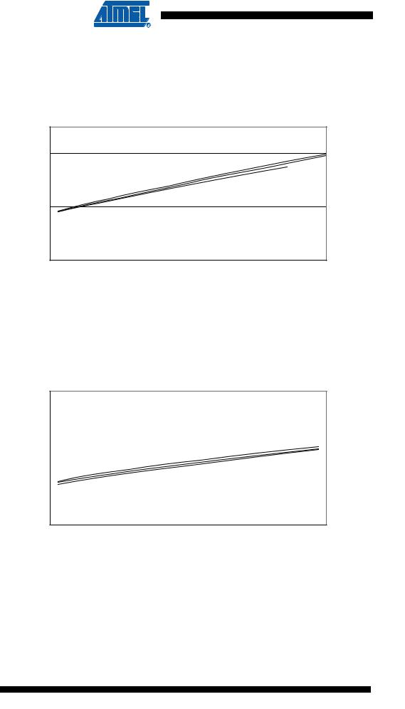
Figure 112. Reset Pin as I/O – Input Threshold Voltage vs. VCC (VIH, Reset Pin Read as “1”)
RESET PIN AS I/O - INPUT THRESHOLD VOLTAGE vs. VCC
Threshold (V)
VIH, RESET PIN READ AS '1'
2.5
-40°C 2 85°C  25°C
25°C
1.5
1
0.5
0
2 |
2.5 |
3 |
3.5 |
4 |
4.5 |
5 |
5.5 |
VCC (V)
Figure 113. Reset Pin as I/O – Input Threshold Voltage vs. VCC (VIL, Reset Pin Read as “0”)
Threshold (V)
RESET PIN AS I/O - INPUT THRESHOLD VOLTAGE vs. VCC
VIL, RESET PIN READ AS '0'
2.5
2
-40°C
1.5  25°C
25°C
85°C
1
0.5
0
2 |
2.5 |
3 |
3.5 |
4 |
4.5 |
5 |
5.5 |
VCC (V)
154 ATtiny26(L)
1477J–AVR–06/07
ATtiny26(L)
Figure 114. Reset Pin as I/O – Pin Hysteresis vs. VCC
RESET PIN AS I/O - PIN HYSTERESIS vs. VCC
|
0.7 |
|
|
|
|
|
|
|
|
0.6 |
|
|
|
|
|
|
|
|
|
|
|
|
|
|
|
85°C |
|
0.5 |
|
|
|
|
|
|
-40°C |
|
|
|
|
|
|
|
|
|
|
|
|
|
|
|
|
|
25°C |
(V) |
0.4 |
|
|
|
|
|
|
|
Threshold |
|
|
|
|
|
|
|
|
0.3 |
|
|
|
|
|
|
|
|
|
|
|
|
|
|
|
|
|
|
0.2 |
|
|
|
|
|
|
|
|
0.1 |
|
|
|
|
|
|
|
|
0 |
|
|
|
|
|
|
|
|
2 |
2.5 |
3 |
3.5 |
4 |
4.5 |
5 |
5.5 |
VCC (V)
Figure 115. Reset Input Threshold Voltage vs. VCC (VIH, Reset Pin Read as “1”)
Threshold (V)
RESET INPUT THRESHOLD VOLTAGE vs. VCC
VIH, RESET PIN READ AS '1'
2.5
2
1.5
-40°C 25°C
85°C
1
0.5
0
1.5 |
2 |
2.5 |
3 |
3.5 |
4 |
4.5 |
5 |
5.5 |
|
|
|
|
VCC (V) |
|
|
|
|
155
1477J–AVR–06/07

Figure 116. Reset Input Threshold Voltage vs. VCC (VIL, Reset Pin Read as “0”)
RESET INPUT THRESHOLD VOLTAGE vs. VCC
VIL, RESET PIN READ AS '0'
|
2.5 |
|
|
|
|
|
|
|
|
2 |
|
|
|
|
|
|
|
(V) |
1.5 |
|
|
|
|
|
|
|
Threshold |
|
85°C |
|
|
|
|
|
|
1 |
25°C |
|
|
|
|
|
|
|
-40°C |
|
|
|
|
|
|
||
|
|
|
|
|
|
|
||
|
|
|
|
|
|
|
|
|
|
0.5 |
|
|
|
|
|
|
|
|
0 |
|
|
|
|
|
|
|
|
2 |
2.5 |
3 |
3.5 |
4 |
4.5 |
5 |
5.5 |
|
|
|
|
|
VCC (V) |
|
|
|
Figure 117. Reset Input Pin Hysteresis vs. VCC
Threshold (V)
0.5
0.45
0.4
0.35
0.3
0.25
0.2
0.15
0.1
0.05
0
2
RESET INPUT PIN HYSTERESIS vs. VCC
-40°C
25°C
85°C
2.5 |
3 |
3.5 |
4 |
4.5 |
5 |
5.5 |
VCC (V)
156 ATtiny26(L)
1477J–AVR–06/07

ATtiny26(L)
BOD Thresholds and Analog Figure 118. BOD Thresholds vs. Temperature (BOD Level is 4.0V)
Comparator Offset
Threshold (V)
BOD THRESHOLDS vs. TEMPERATURE
BODLEVEL IS 4.0V
4.3
4.2
Rising VCC
4.1
4
Falling VCC
3.9
3.8
-50 |
-40 |
-30 |
-20 |
-10 |
0 |
10 |
20 |
30 |
40 |
50 |
60 |
70 |
80 |
90 |
100 |
|
|
|
|
|
|
|
Temperature (C) |
|
|
|
|
|
|
|
|
Figure 119. BOD Thresholds vs. Temperature (BOD Level is 2.7V)
Threshold (V)
BOD THRESHOLDS vs. TEMPERATURE
BODLEVEL IS 2.7V
3.1
3
Rising VCC
2.9
2.8
Falling VCC
2.7
2.6
-50 -40 -30 -20 -10 0 10 20 30 40 50 60 70 80 90 100 Temperature (C)
157
1477J–AVR–06/07

Figure 120. Bandgap Voltage vs. VCC
BANDGAP vs. VCC
Bandgap Voltage (V)
1.236 |
|
|
|
|
|
|
1.234 |
|
|
|
|
|
-40°C |
|
|
|
|
|
|
|
1.232 |
|
|
|
|
|
85°C |
1.23 |
|
|
|
|
|
25°C |
1.228 |
|
|
|
|
|
|
1.226 |
|
|
|
|
|
|
1.224 |
|
|
|
|
|
|
1.222 |
|
|
|
|
|
|
1.22 |
|
|
|
|
|
|
1.218 |
|
|
|
|
|
|
1.216 |
|
|
|
|
|
|
2.5 |
3 |
3.5 |
4 |
4.5 |
5 |
5.5 |
Vcc (V)
Figure 121. Analog Comparator Offset Voltage vs. Common Mode Voltage (VCC= 5.0V)
Comparator Offset Voltage (V)
ANALOG COMPARATOR OFFSET VOLTAGE vs. COMMON MODE VOLTAGE
Vcc = 5V
0.009
0.008
0.007
0.006
0.005
-40°C
0.004
25°C
0.003
85°C
0.002
0.001
0
0 |
1 |
2 |
3 |
4 |
Common Mode Voltage (V)
158 ATtiny26(L)
1477J–AVR–06/07