


AVR CPU Core
Architectural Overview
The fast-access Register File concept contains 32 x 8-bit general purpose working registers with a single clock cycle access time. This means that during one single clock cycle, one ALU (Arithmetic Logic Unit) operation is executed. Two operands are output from the Register File, the operation is executed, and the result is stored back in the Register File – in one clock cycle.
Six of the 32 registers can be used as 16-bit pointers for indirect memory access. These pointers are called the X-, Y-, and Z-pointers, and they can address the Register File and the Flash program memory.
Figure 2. The ATtiny26(L) AVR Enhanced RISC Architecture
1024 x 16 Program FLASH
Instruction
Register
Instruction
Decoder
Control Lines
Program
Counter
Direct Addressing |
Indirect Addressing |
8-bit Data Bus
|
|
|
|
|
|
|
|
|
|
|
|
|
Control |
|
|
|
|
|
|
|
|
|
|
|
|
|
Registers |
|
|
Status |
|
|
|
|
|
|
|
|
|
||
|
|
||||||||||||
|
|
and Test |
|
|
|
|
|
|
|
|
|
||
|
|
|
|
|
|
|
|
|
Interrupt |
||||
|
|
|
|
|
|
|
|
|
|
|
|
|
|
|
|
|
|
|
|
|
|
|
|
|
|
|
|
|
|
32 x 8 |
Unit |
||||||||||
|
|
|
|||||||||||
|
|
|
|||||||||||
|
|
Universal |
|||||||||||
|
|
General |
|
|
Serial Interface |
||||||||
|
|
|
|||||||||||
|
|
Purpose |
|
|
|
|
|
|
|||||
|
|
|
|
|
|
|
|
|
|
||||
|
|
Registers |
|
||||||||||
|
|
ISP Unit |
|||||||||||
|
|
|
|
|
|
|
|
|
|
|
|
|
|
|
|
|
|
|
|
|
|
|
|
|
|
|
|
|
|
|
|
|
|
|
|
|
|
|
|
|
|
|
|
|
|
|
|
|
|
|
|
|
|
|
|
|
|
|
|
|
|
|
|
|
|
|
|
|
|
|
|
|
|
|
|
|
|
|
|
|
|
|
2 x 8-bit |
|
|
ALU |
Timer/Counter |
||||||||||
|
|
|
|||||||||||
|
|
||||||||||||
|
|
|
|
|
|
|
|
|
|
|
|
|
|
|
|
|
|
|
|
|
|
|
|
|
|
|
Watchdog |
|
|
|
|
|
|
|
|
|
|
|
|
|
Timer |
|
|
|
|
|
|
|
|
|
|
|
|
|
|
|
|
|
|
|
|
|
|||||||
|
|
128 x 8 |
|
ADC |
|||||||||
|
|
SRAM |
|
|
|
|
|
|
|
|
|
||
|
|
|
|
||||||||||
|
|
|
|
|
|
|
|
|
|
|
|
|
|
|
|
|
|
|
|
|
|
|
|
|
|
|
|
|
|
128 byte |
|
Analog |
|||||||||
|
|
EEPROM |
|
|
|
|
|
|
|
Comparator |
|||
|
|
|
|
|
|
|
|
|
|
|
|
|
|
I/O Lines
The ALU supports arithmetic and logic functions between registers or between a constant and a register. Single register operations are also executed in the ALU. Figure 2 shows the ATtiny26(L) AVR Enhanced RISC microcontroller architecture. In addition to the register operation, the conventional memory addressing modes can be used on the Register File as well. This is enabled by the fact that the Register File is assigned the 32 lowermost Data Space addresses ($00 - $1F), allowing them to be accessed as though they were ordinary memory locations.
The I/O memory space contains 64 addresses for CPU peripheral functions as Control Registers, Timer/Counters, A/D Converters, and other I/O functions. The I/O Memory can be accessed directly, or as the Data Space locations following those of the Register File, $20 - $5F.
8 ATtiny26(L)
1477J–AVR–06/07

 ATtiny26(L)
General Purpose
Register File
The AVR uses a Harvard architecture concept with separate memories and buses for program and data memories. The program memory is accessed with a two stage pipelining. While one instruction is being executed, the next instruction is pre-fetched from the program memory. This concept enables instructions to be executed in every clock cycle. The program memory is In-System programmable Flash memory.
With the relative jump and relative call instructions, the whole address space is directly accessed. All AVR instructions have a single 16-bit word format, meaning that every program memory address contains a single 16-bit instruction.
During interrupts and subroutine calls, the return address program counter (PC) is stored on the Stack. The Stack is effectively allocated in the general data SRAM, and consequently the stack size is only limited by the total SRAM size and the usage of the SRAM. All user programs must initialize the SP in the reset routine (before subroutines or interrupts are executed). The 8-bit Stack Pointer SP is read/write accessible in the I/O space. For programs written in C, the stack size must be declared in the linker file. Refer to the C user guide for more information.
The 128 bytes data SRAM can be easily accessed through the five different addressing modes supported in the AVR architecture.
The memory spaces in the AVR architecture are all linear and regular memory maps.
The I/O memory space contains 64 addresses for CPU peripheral functions as Control Registers, Timer/Counters, and other I/O functions. The memory spaces in the AVR architecture are all linear and regular memory maps.
A flexible interrupt module has its control registers in the I/O space with an additional Global Interrupt Enable bit in the Status Register. All the different interrupts have a separate Interrupt Vector in the Interrupt Vector table at the beginning of the program memory. The different interrupts have priority in accordance with their Interrupt Vector position. The lower the Interrupt Vector address, the higher the priority.
Figure 3 shows the structure of the 32 general purpose working registers in the CPU.
Figure 3. AVR CPU General Purpose Working Registers
7 |
0 |
Addr. |
|
|
|
|
R0 |
$00 |
|
|
|
|
|
|
|
|
R1 |
$01 |
|
|
|
|
|
|
|
|
R2 |
$02 |
|
|
|
|
|
|
|
|
… |
|
|
|
|
|
|
|
|
|
R13 |
$0D |
|
|
|
|
|
|
General |
|
R14 |
$0E |
|
|
|
|
|
|
Purpose |
|
R15 |
$0F |
|
|
|
|
|
|
Working |
|
R16 |
$10 |
|
|
|
|
|
|
Registers |
|
R17 |
$11 |
|
|
|
|
|
|
|
|
… |
|
|
|
|
|
|
|
|
|
R26 |
$1A |
X-register Low Byte |
|
|
|
|
|
|
|
R27 |
$1B |
X-register High Byte |
|
|
|
|
|
|
|
R28 |
$1C |
Y-register Low Byte |
|
|
|
|
|
|
|
R29 |
$1D |
Y-register High Byte |
|
|
|
|
|
|
|
R30 |
$1E |
Z-register Low Byte |
|
|
|
|
|
|
|
R31 |
$1F |
Z-register High Byte |
|
|
|
|
|
9
1477J–AVR–06/07

All of the register operating instructions in the instruction set have direct and single cycle access to all registers. The only exceptions are the five constant arithmetic and logic instructions SBCI, SUBI, CPI, ANDI, and ORI between a constant and a register, and the LDI instruction for load immediate constant data. These instructions apply to the second half of the registers in the Register File – R16..R31. The general SBC, SUB, CP, AND, and OR, and all other operations between two registers or on a single register apply to the entire Register File.
As shown in Figure 3, each register is also assigned a data memory address, mapping them directly into the first 32 locations of the user Data Space. Although not being physically implemented as SRAM locations, this memory organization provides flexibility in access of the registers, as the X-, Y-, and Z-registers can be set to index any register in the file.
X-register, Y-register, and Z- The registers R26..R31 have some added functions to their general purpose usage. register These registers are address pointers for indirect addressing of the Data Space. The
three indirect address registers X, Y, and Z are defined as:
Figure 4. |
X-, Y-, and Z-register |
|
|
|
|
|
15 |
|
|
0 |
|
X-register |
|
|
|
|
|
|
7 |
0 |
7 |
0 |
|
|
|
R27 ($1B) |
|
R26 ($1A) |
|
|
15 |
|
|
0 |
|
Y-register |
|
7 |
0 |
7 |
0 |
|
|
R29 ($1D) |
|
R28 ($1C) |
|
|
15 |
|
|
0 |
|
Z-register |
|
|
|
|
|
|
7 |
0 |
7 |
0 |
|
|
|
R31 ($1F) |
|
R30 ($1E) |
|
ALU – Arithmetic Logic
Unit
In the different addressing modes, these address registers have functions as fixed displacement, automatic increment and decrement (see the descriptions for the different instructions).
The high-performance AVR ALU operates in direct connection with all 32 general purpose working registers. Within a single clock cycle, ALU operations between registers in the Register File are executed. The ALU operations are divided into three main categories – Arithmetic, Logical, and Bit-functions.
10 ATtiny26(L)
1477J–AVR–06/07
ATtiny26(L)
Status Register – SREG The AVR Status Register – SREG – at I/O space location $3F is defined as:
Bit |
7 |
6 |
5 |
4 |
3 |
2 |
1 |
0 |
|
|
$3F ($5F) |
I |
T |
H |
S |
V |
N |
Z |
C |
SREG |
|
|
|
|
|
|
|
|
|
|
|
|
Read/Write |
R/W |
R/W |
R/W |
R/W |
R/W |
R/W |
R/W |
R/W |
|
|
Initial Value |
0 |
0 |
0 |
0 |
0 |
0 |
0 |
0 |
|
|
• Bit 7 – I: Global Interrupt Enable
The Global Interrupt Enable bit must be set (one) for the interrupts to be enabled. The individual interrupt enable control is then performed in the Interrupt Mask Registers – GIMSK and TIMSK. If the Global Interrupt Enable Register is cleared (zero), none of the interrupts are enabled independent of the GIMSK and TIMSK values. The I-bit is cleared by hardware after an interrupt has occurred, and is set by the RETI instruction to enable subsequent interrupts. The I-bit can also be set and cleared by the application with the SEI and CLI instructions, as described in the instruction set reference.
• Bit 6 – T: Bit Copy Storage
The Bit Copy instructions BLD (Bit LoaD) and BST (Bit STore) use the T-bit as source and destination for the operated bit. A bit from a register in the Register File can be copied into T by the BST instruction, and a bit in T can be copied into a bit in a register in the Register File by the BLD instruction.
• Bit 5 – H: Half Carry Flag
The Half Carry Flag H indicates a Half Carry in some arithmetic operations. See the Instruction Set Description for detailed information.
• Bit 4 – S: Sign Bit, S = N V
The S-bit is always an exclusive or between the Negative Flag N and the Two’s Complement Overflow Flag V. See the Instruction Set Description for detailed information.
• Bit 3 – V: Two’s Complement Overflow Flag
The Two’s Complement Overflow Flag V supports two’s complement arithmetics. See the Instruction Set Description for detailed information.
• Bit 2 – N: Negative Flag
The Negative Flag N indicates a negative result after the different arithmetic and logic operations. See the Instruction Set Description for detailed information.
• Bit 1 – Z: Zero Flag
The Zero Flag Z indicates a zero result after the different arithmetic and logic operations. See the Instruction Set Description for detailed information.
• Bit 0 – C: Carry Flag
The Carry Flag C indicates a carry in an arithmetic or logic operation. See the Instruction
Set Description for detailed information.
11
1477J–AVR–06/07
Stack Pointer – SP
The ATtiny26(L) Stack Pointer is implemented as an 8-bit register in the I/O space location $3D ($5D). As the ATtiny26(L) data memory has 224 ($E0) locations, eight bits are used.
Program and Data
Addressing Modes
Register Direct, Single
Register Rd
Bit |
|
7 |
6 |
5 |
4 |
3 |
2 |
1 |
0 |
|
$3D ($5D) |
SP7 |
SP6 |
SP5 |
SP4 |
SP3 |
SP2 |
SP1 |
SP0 |
SP |
|
|
|
|
|
|
|
|
|
|
|
|
Read/Write |
R/W |
R/W |
R/W |
R/W |
R/W |
R/W |
R/W |
R/W |
|
|
Initial Value |
0 |
0 |
0 |
0 |
0 |
0 |
0 |
0 |
|
|
The Stack Pointer points to the data SRAM stack area where the Subroutine and Interrupt Stacks are located. This Stack space in the data SRAM must be defined by the program before any subroutine calls are executed or interrupts are enabled. The Stack Pointer must be set to point above $60. The Stack Pointer is decremented by one when data is pushed onto the Stack with the PUSH instruction, and it is decremented by two when an address is pushed onto the Stack with subroutine calls and interrupts. The Stack Pointer is incremented by one when data is popped from the Stack with the POP instruction, and it is incremented by two when an address is popped from the Stack with return from subroutine RET or return from interrupt RETI.
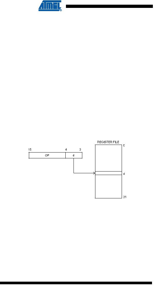
The ATtiny26(L) AVR Enhanced RISC microcontroller supports powerful and efficient addressing modes for access to the Flash program memory, SRAM, Register File, and I/O Data memory. This section describes the different addressing modes supported by the AVR architecture. In the figures, OP means the operation code part of the instruction word. To simplify, not all figures show the exact location of the addressing bits.
Figure 5. Direct Single Register Addressing
The operand is contained in register d (Rd).
12 ATtiny26(L)
1477J–AVR–06/07