

 ATtiny26(L)
Figure 86. Idle Supply Current vs. VCC (32 kHz External Oscillator)
ICC (uA)
IDLE SUPPLY CURRENT vs. VCC
32kHz EXTERNAL OSCILLATOR
30
 25°C
25°C
25
20
15
10
5
0
2 |
2.5 |
3 |
3.5 |
4 |
4.5 |
5 |
5.5 |
VCC (V)
Power-down Supply Current |
Figure 87. Power-down Supply Current vs. VCC (Watchdog Timer Disabled) |
ICC (uA)
POWER-DOWN SUPPLY CURRENT vs. VCC
WATCHDOG TIMER DISABLED
1.8
85°C
1.6
1.4
-40°C
1.2
25°C
1
0.8
0.6
0.4
0.2
0
2 |
2.5 |
3 |
3.5 |
4 |
4.5 |
5 |
5.5 |
VCC (V)
141
1477J–AVR–06/07

Figure 88. Power-down Supply Current vs. VCC (Watchdog Timer Enabled)
ICC (uA)
POWER-DOWN SUPPLY CURRENT vs. VCC
WATCHDOG TIMER ENABLED
20 |
85°C |
|
|
||
18 |
25°C |
|
-40°C |
||
|
||
16 |
|
14
12
10
8
6
4
2
0
2 |
2.5 |
3 |
3.5 |
4 |
4.5 |
5 |
5.5 |
VCC (V)
Standby Supply Current |
Figure 89. Standby Supply Current vs. VCC (455 kHz Resonator, Watchdog Timer |
|
Disabled) |
ICC (uA)
STANDBY SUPPLY CURRENT vs. VCC
455 kHz RESONATOR, WATCHDOG TIMER DISABLED
70
60
50
40
30
20
10
0
2 |
2.5 |
3 |
3.5 |
4 |
4.5 |
5 |
5.5 |
VCC (V)
142 ATtiny26(L)
1477J–AVR–06/07

 ATtiny26(L)
Figure 90. Standby Supply Current vs. VCC (1 MHz Resonator, Watchdog Timer
Disabled)
STANDBY SUPPLY CURRENT vs. VCC
1 MHz RESONATOR, WATCHDOG TIMER DISABLED
60
50
ICC (uA)
40
30
20
10
0
2 |
2.5 |
3 |
3.5 |
4 |
4.5 |
5 |
5.5 |
VCC (V)
Figure 91. Standby Supply Current vs. VCC (2 MHz Resonator, Watchdog Timer Disabled)
STANDBY SUPPLY CURRENT vs. VCC
2 MHz RESONATOR, WATCHDOG TIMER DISABLED
80
70
ICC (uA)
60
50
40
30
20
10
0
2 |
2.5 |
3 |
3.5 |
4 |
4.5 |
5 |
5.5 |
VCC (V)
143
1477J–AVR–06/07

Figure 92. Standby Supply Current vs. VCC (2 MHz XTAL, Watchdog Timer Disabled)
ICC (uA)
STANDBY SUPPLY CURRENT vs. VCC
2 MHz XTAL, WATCHDOG TIMER DISABLED
90
80
70
60
50
40
30
20
10
0
2 |
2.5 |
3 |
3.5 |
4 |
4.5 |
5 |
5.5 |
VCC (V)
Figure 93. Standby Supply Current vs. VCC (4 MHz Resonator, Watchdog Timer Disabled)
STANDBY SUPPLY CURRENT vs. VCC
4 MHz RESONATOR, WATCHDOG TIMER DISABLED
120
100
80
ICC (uA)
60
40
20
0
2 |
2.5 |
3 |
3.5 |
4 |
4.5 |
5 |
5.5 |
VCC (V)
144 ATtiny26(L)
1477J–AVR–06/07
 ATtiny26(L)
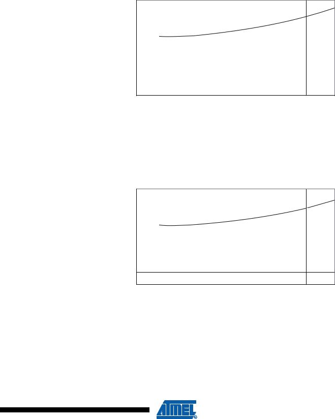
Figure 94. Standby Supply Current vs. VCC (4 MHz XTAL, Watchdog Timer Disabled)
ICC (uA)
STANDBY SUPPLY CURRENT vs. VCC
4 MHz XTAL, WATCHDOG TIMER DISABLED
120
100
80
60
40
20
0
2 |
2.5 |
3 |
3.5 |
4 |
4.5 |
5 |
5.5 |
VCC (V)
Figure 95. Standby Supply Current vs. VCC (6 MHz Resonator, Watchdog Timer Disabled)
STANDBY SUPPLY CURRENT vs. VCC
6 MHz RESONATOR, WATCHDOG TIMER DISABLED
160
ICC (uA)
140
120
100
80
60
40
20
0
2 |
2.5 |
3 |
3.5 |
4 |
4.5 |
5 |
5.5 |
VCC (V)
145
1477J–AVR–06/07