

- •Features
- •Pin Configuration
- •Description
- •Block Diagram
- •Pin Descriptions
- •AVCC
- •Port A (PA7..PA0)
- •Port B (PB7..PB0)
- •XTAL1
- •XTAL2
- •Resources
- •AVR CPU Core
- •Architectural Overview
- •I/O Direct
- •Data Direct
- •Data Indirect with Displacement
- •Data Indirect
- •Memories
- •SRAM Data Memory
- •EEPROM Data Memory
- •EEPROM Read/Write Access
- •I/O Memory
- •Clock Systems and their Distribution
- •Clock Sources
- •Default Clock Source
- •Crystal Oscillator
- •External RC Oscillator
- •External Clock
- •Power-on Reset
- •External Reset
- •Brown-out Detection
- •Watchdog Reset
- •Idle Mode
- •Power-down Mode
- •Standby Mode
- •Analog to Digital Converter
- •Analog Comparator
- •Brown-out Detector
- •Internal Voltage Reference
- •Watchdog Timer
- •Port Pins
- •I/O Ports
- •Introduction
- •Configuring the Pin
- •Reading the Pin Value
- •Unconnected Pins
- •Alternate Port Functions
- •Alternate Functions of Port A
- •Alternate Functions Of Port B
- •Register Description for I/O Ports
- •Interrupts
- •Interrupt Vectors
- •Interrupt Handling
- •Interrupt Response Time
- •External Interrupt
- •Pin Change Interrupt
- •Timer/Counters
- •Timer/Counter0 Prescaler
- •Timer/Counter1 Prescaler
- •8-bit Timer/Counter0
- •8-bit Timer/Counter1
- •Timer/Counter1 in PWM Mode
- •Watchdog Timer
- •Overview
- •Register Descriptions
- •Functional Descriptions
- •Three-wire Mode
- •SPI Slave Operation Example
- •Two-wire Mode
- •Start Condition Detector
- •Alternative USI Usage
- •4-bit Counter
- •12-bit Timer/Counter
- •Software Interrupt
- •Analog Comparator
- •Analog to Digital Converter
- •Features
- •Operation
- •Changing Channel or Reference Selection
- •ADC Conversion Result
- •ADLAR = 0
- •ADLAR = 1
- •Fuse Bits
- •Latching of Fuses
- •Signature Bytes
- •Calibration Byte
- •Page Size
- •Signal Names
- •Parallel Programming
- •Enter Programming Mode
- •Chip Erase
- •Programming the Flash
- •Programming the EEPROM
- •Reading the Flash
- •Reading the EEPROM
- •Programming the Lock Bits
- •Reading the Signature Bytes
- •Reading the Calibration Byte
- •Serial Downloading
- •Data Polling Flash
- •Data Polling EEPROM
- •Electrical Characteristics
- •Absolute Maximum Ratings*
- •DC Characteristics
- •External Clock Drive Waveforms
- •External Clock Drive
- •ADC Characteristics
- •Active Supply Current
- •Idle Supply Current
- •Power-down Supply Current
- •Standby Supply Current
- •Pin Pull-up
- •Internal Oscillator Speed
- •Register Summary
- •Instruction Set Summary
- •Ordering Information
- •Packaging Information
- •Errata
- •ATtiny26 Rev. B/C/D
- •Table of Contents

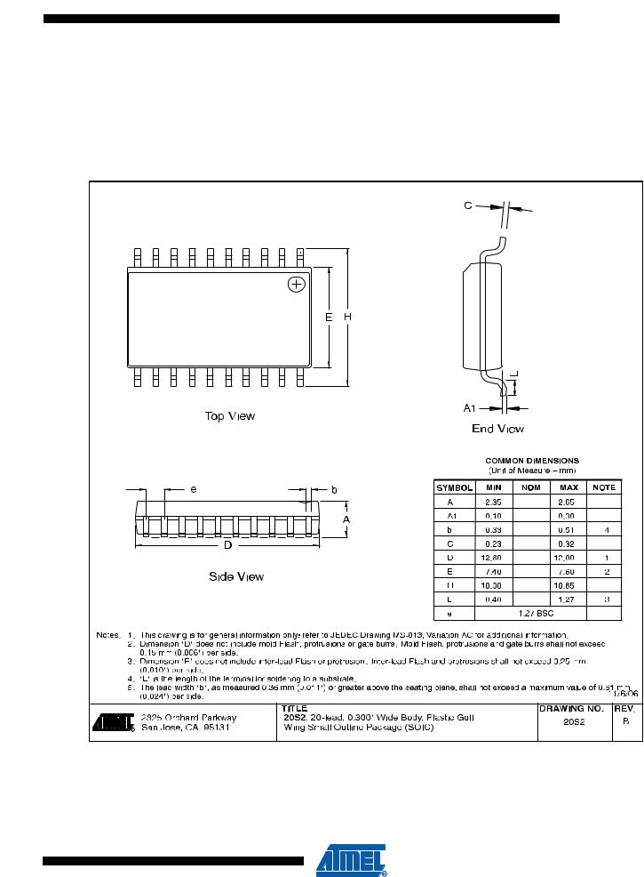
Packaging Information
20P3
D
PIN 1
E1
A
SEATING PLANE
A1
L
B
B1
e
E
C 
 eC
eC
eB
Notes: 1. This package conforms to JEDEC reference MS-001, Variation AD.
2.Dimensions D and E1 do not include mold Flash or Protrusion. Mold Flash or Protrusion shall not exceed 0.25 mm (0.010").
COMMON DIMENSIONS
(Unit of Measure = mm)
SYMBOL |
MIN |
NOM |
MAX |
NOTE |
A |
– |
– |
5.334 |
|
A1 |
0.381 |
– |
– |
|
D |
25.493 |
– |
25.984 |
Note 2 |
E |
7.620 |
– |
8.255 |
|
E1 |
6.096 |
– |
7.112 |
Note 2 |
B |
0.356 |
– |
0.559 |
|
B1 |
1.270 |
– |
1.551 |
|
L |
2.921 |
– |
3.810 |
|
C |
0.203 |
– |
0.356 |
|
eB |
– |
– |
10.922 |
|
eC |
0.000 |
– |
1.524 |
|
|
|
|
|
|
e |
|
2.540 TYP |
|
|
1/12/04
TITLE
|
2325 Orchard Parkway |
20P3, 20-lead (0.300"/7.62 mm Wide) Plastic Dual |
|
San Jose, CA 95131 |
|
R |
Inline Package (PDIP) |
DRAWING NO. REV.
20P3 C
174 ATtiny26(L)
1477J–AVR–06/07
ATtiny26(L)
20S
175
1477J–AVR–06/07

32M1-A

 D
D 


 D1
D1 

1 |
0 |
|
2 |
||
Pin 1 ID |
||
3 |
E1 
 E
E
TOP VIEW
A2 
A
 K
K
P |
|
|
D2 |
|
|
P |
1 |
|
2 |
||
Pin #1 Notch |
||
|
(0.20 R) 3
E2
K
b |
e |
L |
BOTTOM VIEW
Note: JEDEC Standard MO-220, Fig. 2 (Anvil Singulation), VHHD-2.
SIDE VIEW

 A3
A3


 A1
A1

 0.08 C COMMON DIMENSIONS
(Unit of Measure = mm)
SYMBOL |
MIN |
NOM |
MAX |
NOTE |
A |
0.80 |
0.90 |
1.00 |
|
|
|
|
|
|
A1 |
– |
0.02 |
0.05 |
|
|
|
|
|
|
A2 |
– |
0.65 |
1.00 |
|
|
|
|
|
|
A3 |
|
0.20 REF |
|
|
|
|
|
|
|
b |
0.18 |
0.23 |
0.30 |
|
|
|
|
|
|
D |
4.90 |
5.00 |
5.10 |
|
|
|
|
|
|
D1 |
4.70 |
4.75 |
4.80 |
|
|
|
|
|
|
D2 |
2.95 |
3.10 |
3.25 |
|
|
|
|
|
|
E |
4.90 |
5.00 |
5.10 |
|
|
|
|
|
|
E1 |
4.70 |
4.75 |
4.80 |
|
|
|
|
|
|
E2 |
2.95 |
3.10 |
3.25 |
|
|
|
|
|
|
e |
|
0.50 BSC |
|
|
|
|
|
|
|
L |
0.30 |
0.40 |
0.50 |
|
|
|
|
|
|
P |
– |
– |
0.60 |
|
|
|
|
|
|
0 |
– |
– |
12o |
|
K |
0.20 |
– |
– |
|
|
|
|
|
|
5/25/06
TITLE
|
2325 Orchard Parkway |
32M1-A, 32-pad, 5 x 5 x 1.0 mm Body, Lead Pitch 0.50 mm, |
|
San Jose, CA 95131 |
|
R |
3.10 mm Exposed Pad, Micro Lead Frame Package (MLF) |
DRAWING NO. REV.
32M1-A E
176 ATtiny26(L)
1477J–AVR–06/07