

Micro-Cap v7.1.6 / Ug
.pdfWhile the Component menu hierarchical structure provides easy access to parts, it can take several steps to find the one you want. A fast way to select frequently used parts is the Component palette. These user-selected parts palettes can be toggled on and off with a single key. You click on the part you want, then leave the palette on the screen or make it disappear with the same key that invoked it. The palettes, numbered 1 to 9, are toggled on and off with CTRL + number. Membership in a palette is specified with the Component editor. For example, CTRL + 1 toggles palette 1 on and off.
We'll use a palette to add a resistor. Press CTRL + 1 to invoke palette 1. The screen should now something look like this:
Use spacebar to toggle between the current mode and the Select mode
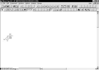
Figure 3-5 A user palette
Click on the Resistor name in the palette. Press CTRL + 1 to remove the palette. Drag the resistor to the source and rotate it until it is horizontal. When one of the resistor leads is just touching the top of the source, release the mouse button. If the Node Snap option is on, the resistor lead only needs to be near the source. The resistor lead will snap to the nearest node. Release the mouse button, and the Attribute dialog box will appear. MC7 suggests the name R1 which we'll accept. Type "1K" for the VALUE attribute, and press ENTER.
Let's move the resistor attribute text. To move anything we must be in Select mode. To activate Select mode, click on the Select mode button  in the upper
left portion of the Tool bar, or simply press SPACEBAR. Drag the resistor name, R1, and its value 1K, until they are centered, respectively, above and below the resistor body. Attribute text can be moved relative to the part by simply dragging it to the desired position. The initial position of attribute text relative to the shape is
65
determined in the Component library. After the part is placed, its text attributes (e.g. NAME and VALUE) can be moved as desired. Attribute visibility can also be toggled on and off from the Attribute dialog box.
|
|
|
|
|
|
|
|
|
|
|
|
|
|
|
|
|
|
|
Figure 3-6 The circuit after moving the value attribute |
||||
|
Select Analog Library / BJT / 2N0000- / 2N3903- / 2N4013 from the Com- |
||||
|
|||||
Select a new |
ponent menu. This selects the 2N4013, a pre-modeled bipolar NPN transistor. |
||||
part from the |
Drag the NPN so that its emitter points down and its base touches the right resis- |
||||
Component |
tor lead. Click the mouse button. The Attribute dialog box does not appear since |
||||
menu or User |
all of the parts in the Analog Library and Digital Library groups have their As- |
||||
palette only if the |
sign Component Name to MODEL flag set. This sets the MODEL attribute |
||||
part is different |
to the component name. When you select the part name 2N4013, the model name |
||||
from the last one |
is known to be the same, and its model parameters are readily available in the |
||||
chosen. |
model libraries. Since the part name and model name are already known, the dia- |
||||
|
log box isn't needed and doesn't appear. It is easier to use a part from the Analog |
||||
|
Library and Digital Library sections of the Component menu than from the Ana- |
||||
|
log Primitives and Digital Primitives sections. You simply pick a part from the |
||||
|
library and drop it into the schematic. No modeling decisions are required. Com- |
||||
|
ponents chosen from the Analog Primitives and Digital Primitives portion of the |
||||
|
library, like the Pulse Source, require a specific model name and parameter set, |
||||
|
which may be selected from the libraries or entered by editing if desired. |
||||
|
Invoke palette 1 again with CTRL + 1. Select Resistor from the palette. Click in |
||||
|
the schematic and add a 10K resistor. Point it up from the collector lead. Select |
||||
|
Battery from the palette and place a battery vertically so that its positive lead |
||||
|
touches the top resistor lead. Set its value to 10. From the palette, select Ground. |
||||
|
Place a ground vertically with its lead touching the negative battery lead. Add |
||||
66 Chapter 3: Creating and Editing Simple Circuits

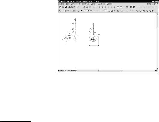
grounds to the emitter and to the pulse source minus lead. Toggle the palette off with CTRL +1. The circuit should now look like Figure 3-7.
Wire mode lets you connect components by dragging the mouse to create a wire.
Figure 3-7 The circuit after adding the bipolar stage
To illustrate a third way to select parts, select the Find Component command from the Component menu or press SHIFT + CTRL + F. Enter OPO8_AD. Click on the Find and OK buttons. Place the opamp to the right of the NPN.
To illustrate a fourth method of part selection, click on the battery  button in the middle of the top row of the Tool bar. Click in the schematic and place a 4.0 volt battery vertically so that its positive lead touches the '99' or 'VCC' lead of the OP08_AD. Click on the ground
  button in the Tool bar. Place a ground at the negative lead of this battery and at the '50' or 'VEE' lead of the OP08_AD.
For a wire to connect two leads together, the endpoints must terminate on a lead or a wire connected to a component lead. To see where the leads are, click on the Pin Connections  button. This draws a small dot at each component lead. You can also display pin names and connections individually for each component by enabling the Display Pin Names option from the Attribute dialog box.
Click on the Wire mode button  in the Tool bar or press CTRL + W. This changes the mode so that dragging the mouse draws a wire. Place the mouse at the '3' or 'plus input' lead. Click the mouse button, and while holding it down, drag the mouse horizontally to the left until the wire touches the junction between the collector lead and the resistor lead. Release the mouse button. This connects the two leads together.
67
Connect the '2' or 'minus input' lead to the '45' or 'output' lead by clicking near the output lead and dragging a wire straight down until it is below the opamp. While still holding the button down, drag the mouse to the left until it is just below the '2' lead. Release the mouse. This creates a right-angled wire extending from the output to an intermediate point below the input lead. Click again at this intermediate point to start a second wire. Drag it to the '2' lead, and release the mouse.
Text mode lets you place grid text anywhere in the schematic. Grid text is mainly used to name nodes. Text is not case sensitive. 1u is the same as 1U.
Figure 3-8 The circuit after wiring the OP08
From the Component menu / Digital Library / 74xx00- / 04- / 7404, select the 7404 buffer. Place the buffer horizontally so that its input lead is to the right of the OP08. Draw a wire from the OP08 output lead to the 7404 input lead. Draw another wire from the 7404 output lead horizontally to the right. Finally, draw the final wire from the pulse source plus lead horizontally to the left.
Click on the Text mode button  or press CTRL + T to enter Text mode. This mode lets us add text to the schematic. Text placed directly on nodes gives the node a name which can be used to refer to it when plotting its node voltage or digital state.
Click on the horizontal wire just added to the pulse source. When the dialog box comes up, type "IN" and click on the OK button. The lower edge of the selection box outlining the text "IN" should just touch the wire. If it doesn't touch, enable the Select mode and drag the text until it does touch. Add the text "A" to the wire connecting the NPN collector to the OP08 plus input lead. Add the text "C" to the wire connected to the 7404 output.
68 Chapter 3: Creating and Editing Simple Circuits
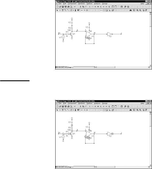
The circuit should now look like Figure 3-9.
Node names and numbers
Figure 3-9 The completed circuit
MC7 assigns node numbers to every analog and digital node to identify them. To see the node numbers, click on the Node Numbers button  in the Tool bar. The circuit should look like this:
Figure 3-10 Node numbers
The program automatically assigns numbers to the circuit nodes when an analysis is requested or when the circuit is saved to disk. It displays them on the schematic only when the Node Numbers option is enabled. When you want to plot or print a node's voltage waveform you refer to the waveform as V(node name), where the
69
node name may be either the node number assigned by the program or a text name assigned by you.
For the program to know about node names, they must be placed directly on the node. The lower left corner of the text outline box must be placed directly on the node. Node Snap, if enabled, makes this easier by moving the text to the nearest node within one grid. The Node Snap option is selected from Options menu /
Preferences / Common Options / Circuit.
The system assigns and displays node numbers according to the following rules:
1.Ground is node number 0, but its node number is never displayed.
2.The other nodes are numbered from 1 to the highest node number.
3.When an analog node and a digital node touch, or are connected by a wire, each node is assigned a unique number. MC7 automatically inserts an interface circuit between the two nodes. The interface circuit creates an interface node of the form <num>$ATOD or <num>$DTOA depending upon whether the digital node is an input or an output, respectively. If the interface node is accessible (can be referenced in a plot expression), it will be printed on the schematic. In general, interface nodes between analog parts and digital primitives are accessible unless they occur at a subcircuit interface. Since the interface node in this circuit occurs at a subcircuit interface it isn't accessible.
4.Analog node numbers are displayed in a box with rounded corners while digital node numbers are displayed in a box with square corners.
5.Nodes with the same text node name are connected together. This is done to provide a convenient way of connecting large numbers of common nodes.
Save this circuit using the Save As option from the File menu. Type "TUTOR" in the file name field. Remove the circuit by selecting Close from the File menu.
70 Chapter 3: Creating and Editing Simple Circuits
Editing component parameters and text
Schematics are composed of components, text, graphical objects, picture files, and wires. To edit any of these items, the item must be selected. To select an item, MC7 must be in the Select mode. To enable the Select mode, press CTRL + E,
click the Select  button in the Tool bar, or press SPACEBAR.
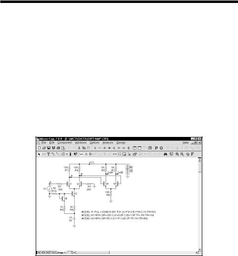
Once in the Select mode, objects or regions can be selected for editing, moving, or deleting. To illustrate, load the sample circuit DIFFAMP and click on the Select button in the Tool bar. Move the mouse to the 6V battery in the upper right part of the schematic. Click the mouse in the center of the battery. This selects and redraws the battery. The display mode, Select or Block Select, can be changed through the Preferences dialog box. The Select or Block Select color can be changed in the Properties dialog box (F10).
Figure 3-11 Selecting the battery for editing
Double-clicking on a selected component activates the Attribute dialog box which lets you edit its attributes. Double click on the battery. MC7 presents the dialog box showing the value attribute 6V and awaits your edits. Type "6.5". Click OK. That's how you change the parameter of this simple part.
To change the forward beta of a transistor simply double-click on the device and when the Attribute dialog box comes up, edit the BF parameter. Editing always localizes the parameters. If a transistor's model parameters are global, editing will make them local. Mechanically, localization is implemented by placing a model statement with the edited parameters in the text area of the circuit.
71

To illustrate, double-click on the Q5 transistor. This invokes the Attribute dialog box which should look like this:
Figure 3-12 Editing model parameters in the Attribute dialog box
In this case, MC7 searched for Q5's model statement, N1, and displayed it in the edit area of the dialog box. When searching for the model statement, MC7 first looks in the schematic and text area. If it doesn't find it there, it looks in libraries referenced by a .LIB statement, including the default master index, NOM.LIB. If it still doesn't find the model statement, it makes one up from default parameter values and copies it to the text area.
After locating the model statement (or creating a suitable default), MC7 displays the parameter values in the edit fields. You can scroll through the parameter values, editing them as you wish. When you click OK, MC7 updates your local copy of the model statement. The program never modifies any libraries as a result of these edits. It only modifies model statements local to the circuit.
You can click on any model name in the Model list box. Selecting one of these by clicking on it will change the part's model name attribute The Cancel button cancels any changes made with the dialog box.
Click the Cancel button.
72 Chapter 3: Creating and Editing Simple Circuits

Clear saves clipboard contents. Cut replaces clipboard contents with deleted objects.
Deleting objects
We can now edit text and component parameters. How about deleting objects? Like editing, deleting requires that the objects be selected. Once selected, they can be deleted with one of two commands; Cut and Clear. Clear, activated by the Del key, deletes without copying to the clipboard. Cut, activated by CTRL + X, deletes and copies to the clipboard. To illustrate, select the pulse source in the DIFFAMP circuit by clicking it. As usual the program colors it to show that it is selected. Press the Del key and the program removes the source.
Undoing and redoing operations
MC7 provides multistage undo and redo functions to reverse the effects of schematic edits and a simple one-stage undo function for most text fields. To illustrate, press CTRL + Z to undo the deletion. The source, which we just deleted, reappears. Press CTRL + Y to redo the change and the source disappears again.
The clipboard
MC7 maintains two clipboards for temporary storage. One is for schematics and the other is for text fields. There are two important clipboard operations.
To copy something to the clipboard, select it, then press CTRL + C.
To paste the contents of the clipboard to a schematic, click the mouse on the schematic at the desired insertion point and press CTRL + V. The clipboard contents are then copied to the schematic and selected. They can be moved by dragging on any selected object in the group. Clicking on any deselected object deselects all objects.
To illustrate, click on the Select button  in the Tool bar. Place the mouse at
the upper left of the second differential stage of the DIFFAMP circuit. Drag the mouse to the lower right until the display looks like Figure 3-13. Upon release of the mouse button, objects originating inside the outline box are selected. Objects originating outside the box are not selected.
73
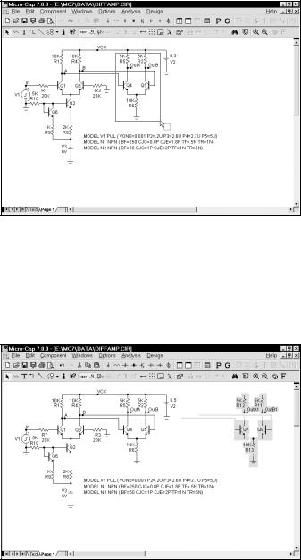
Figure 3-13 Selecting a region for copying to the clipboard
Now press CTRL + C to copy the selected region to the clipboard. Move the mouse to the right of the battery and click the left button. This moves the insertion point. Press CTRL + V to paste the contents of the clipboard to the insertion point. Your circuit should now look like this:
Figure 3-14 After pasting the clipboard contents
The saved region has been copied, or pasted, from the clipboard to the schematic.
74 Chapter 3: Creating and Editing Simple Circuits