

External Reset |
|
|
|
|
|
|
|
|
|
|
|
|
|
|
|
|
|
|
|
|
|
|
|
|
|
|
|
|
|
|
|
|
|
|
|
|
|
|
|
|
|
|
|
|
|
|
|
|
|
|
|
|
|
|
|
|
|
|
|
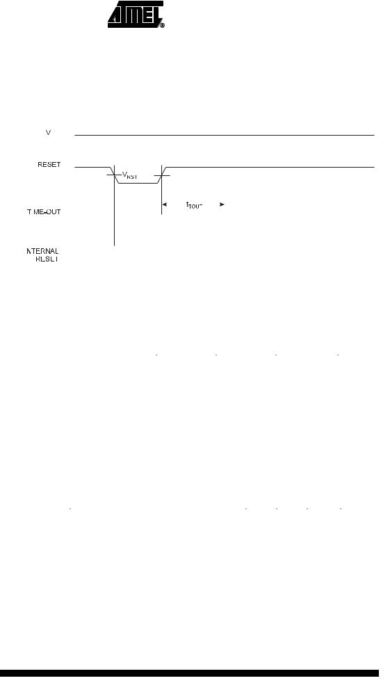
An External Reset is generated by a low level on the RESET pin if enabled. Reset |
|||||||||||||||||||
|
pulses longer than the minimum pulse width (see Table 12) will generate a reset, even if |
||||||||||||||||||
|
the clock is not running. Shorter pulses are not guaranteed to generate a reset. When |
||||||||||||||||||
|
the applied signal reaches the Reset Threshold Voltage – VRST – on its positive edge, |
||||||||||||||||||
|
the delay counter starts the MCU after the Time-out period – tTOUT – has expired. |
||||||||||||||||||
|
Figure 16. External Reset During Operation |
||||||||||||||||||
|
|
|
|
CC |
|||||||||||||||
|
|
|
|
|
|
|
|
|
|
|
|
|
|
|
|
|
|
|
|
|
|
|
|
|
|
|
|
|
|
|
|
|
|
|
|
|
|
|
|
|
|
|
|
|
|
|
|
|
|
|
|
|
|
|
|
|
|
|
|
|
|
|
|
|
|
|
|
|
|
|
|
|
|
|
|
|
|
|
|
|
|
|
|
|
|
|
|
|
|
|
|
|
|
|
|
|
|
|
|
|
|
|
|
|
|
|
|
|
|
|
|
|
|
|
|
|
|
|
|
|
|
|
|
|
|
|
|
|
|
|
|
|
|
|
|
|
|
|
|
|
|
|
|
|
|
|
|
|
|
|
|
|
|
|
|
|
|
|
|
Brown-out Detection |
ATtiny13 has an On-chip Brown-out Detection (BOD) circuit for monitoring the VCC level |
||||
|
during operation by comparing it to a fixed trigger level. The trigger level for the BOD |
||||
|
can be selected by the BODLEVEL Fuses. The trigger level has a hysteresis to ensure |
||||
|
spike free Brown-out Detection. The hysteresis on the detection level should be inter- |
||||
|
preted as VBOT+ = VBOT + VHYST/2 and VBOT- = VBOT - VHYST/2. |
|
|
||
|
Table 13. BODLEVEL Fuse Coding(1) |
|
|
|
|
|
BODLEVEL [1..0] Fuses |
Min VBOT |
Typ VBOT |
Max VBOT |
Units |
|
11 |
|
BOD Disabled |
|
|
|
|
|
|
|
|
|
10 |
|
1.8 |
|
|
|
|
|
|
|
|
|
01 |
|
2.7 |
|
V |
|
|
|
|
|
|
|
00 |
|
4.3 |
|
|
|
|
|
|
|
|
|
Note: 1. VBOT may be below nominal minimum operating voltage for some devices. For |
||||
|
devices where this is the case, the device is tested down to VCC = VBOT during the |
||||
|
production test. This guarantees that a Brown-out Reset will occur before VCC drops |
||||
|
to a voltage where correct operation of the microcontroller is no longer guaranteed. |
||||
Table 14. Brown-out Characteristics
Symbol |
Parameter |
Min |
Typ |
Max |
Units |
|
|
|
|
|
|
VHYST |
Brown-out Detector Hysteresis |
|
50 |
|
mV |
tBOD |
Min Pulse Width on Brown-out Reset |
|
2 |
|
µs |
When the BOD is enabled, and VCC decreases to a value below the trigger level (VBOT- in Figure 17), the Brown-out Reset is immediately activated. When VCC increases above
the trigger level (VBOT+ in Figure 17), the delay counter starts the MCU after the Timeout period tTOUT has expired.
The BOD circuit will only detect a drop in VCC if the voltage stays below the trigger level for longer than tBOD given in Table 12.
32 ATtiny13
2535A–AVR–06/03
 ATtiny13
Figure 17. Brown-out Reset During Operation
VCC |
VBOT+ |
|
VBOT- |
RESET |
|
TIME-OUT |
tTOUT |
INTERNAL |
|
RESET |
|
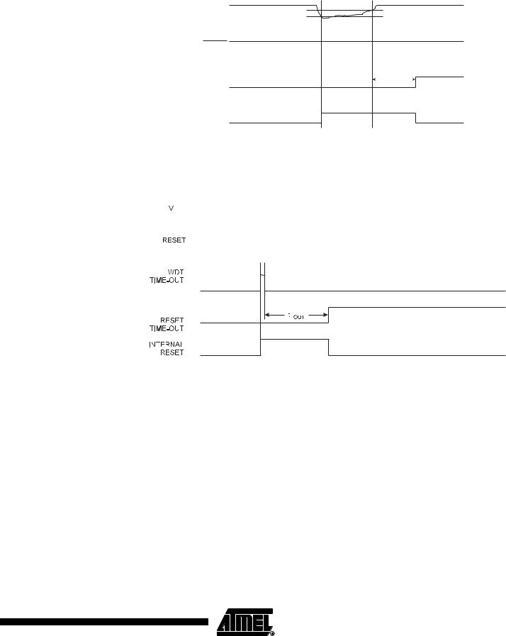
Watchdog Reset |
When the Watchdog times out, it will generate a short reset pulse of one CK cycle dura- |
||||
|
tion. On the falling edge of this pulse, the delay timer starts counting the Time-out period |
||||
|
tTOUT. Refer to page 35 for details on operation of the Watchdog Timer. |
||||
|
Figure 18. Watchdog Reset During Operation |
||||
|
|
CC |
|
|
|
|
|
||||
|
|
|
|
|
|
|
|
|
|
|
|


 CK
CK 

MCU Status Register – |
The MCU Status Register provides information on which reset source caused an MCU |
|||||||||
MCUSR |
Reset. |
|
|
|
|
|
|
|
|
|
|
Bit |
7 |
6 |
5 |
4 |
3 |
2 |
1 |
0 |
|
|
|
|
|
|
|
|
|
|
|
|
|
|
– |
– |
– |
– |
WDRF |
BORF |
EXTRF |
PORF |
MCUSR |
|
|
|
|
|
|
|
|
|
|
|
|
Read/Write |
R |
R |
R |
R |
R/W |
R/W |
R/W |
R/W |
|
|
Initial Value |
0 |
0 |
0 |
0 |
|
See Bit Description |
|
|
|
• Bits 7..4 – Res: Reserved Bits
These bits are reserved bits in the ATtiny13 and will always read as zero.
• Bit 3 – WDRF: Watchdog Reset Flag
This bit is set if a Watchdog Reset occurs. The bit is reset by a Power-on Reset, or by writing a logic zero to the flag.
• Bit 2 – BORF: Brown-out Reset Flag
This bit is set if a Brown-out Reset occurs. The bit is reset by a Power-on Reset, or by writing a logic zero to the flag.
33
2535A–AVR–06/03

|
|
|
|
|
|
|
|
|
|
|
|
|
• Bit 1 – EXTRF: External Reset Flag |
||||
|
This bit is set if an External Reset occurs. The bit is reset by a Power-on Reset, or by |
||||
|
writing a logic zero to the flag. |
||||
|
• Bit 0 – PORF: Power-on Reset Flag |
||||
|
This bit is set if a Power-on Reset occurs. The bit is reset only by writing a logic zero to |
||||
|
the flag. |
||||
|
To make use of the Reset Flags to identify a reset condition, the user should read and |
||||
|
then reset the MCUSR as early as possible in the program. If the register is cleared |
||||
|
before another reset occurs, the source of the reset can be found by examining the |
||||
|
Reset Flags. |
||||
Internal Voltage |
ATtiny13 features an internal bandgap reference. This reference is used for Brown-out |
||||
Reference |
Detection, and it can be used as an input to the Analog Comparator or the ADC. |
||||
Voltage Reference Enable The voltage reference has a start-up time that may influence the way it should be used. Signals and Start-up Time The start-up time is given in Table 15. To save power, the reference is not always turned on. The reference is on during the following situations:
1.When the BOD is enabled (by programming the BODLEVEL [1..0] Fuse).
2.When the bandgap reference is connected to the Analog Comparator (by setting the ACBG bit in ACSR).
3.When the ADC is enabled.
Thus, when the BOD is not enabled, after setting the ACBG bit or enabling the ADC, the user must always allow the reference to start up before the output from the Analog Comparator or ADC is used. To reduce power consumption in Power-down mode, the user can avoid the three conditions above to ensure that the reference is turned off before entering Power-down mode.
Table 15. Internal Voltage Reference Characteristics(1)
Symbol |
Parameter |
Condition |
Min |
Typ |
Max |
Units |
|
|
|
|
|
|
|
VBG |
Bandgap reference voltage |
VCC = 2.7V, |
1.0 |
1.1 |
1.2 |
V |
|
TA = 25°C |
|||||
|
|
|
|
|
|
|
tBG |
Bandgap reference start-up time |
VCC = 2.7V, |
|
40 |
70 |
µs |
|
TA = 25°C |
|
||||
|
|
|
|
|
|
|
IBG |
Bandgap reference current |
VCC = 2.7V, |
|
15 |
|
µA |
consumption |
TA = 25°C |
|
|
|||
|
|
|
|
|
||
Note: 1. |
Values are guidelines only. Actual values are TBD. |
|
|
|
|
|
34 ATtiny13
2535A–AVR–06/03