

Depending of the mode of operation used, the counter is cleared, incremented, or decremented at each timer clock (clkT0). clkT0 can be generated from an external or internal clock source, selected by the Clock Select bits (CS02:0). When no clock source is selected (CS02:0 = 0) the timer is stopped. However, the TCNT0 value can be accessed by the CPU, regardless of whether clkT0 is present or not. A CPU write overrides (has priority over) all counter clear or count operations.
The counting sequence is determined by the setting of the WGM01 and WGM00 bits located in the Timer/Counter Control Register (TCCR0A) and the WGM02 bit located in the Timer/Counter Control Register B (TCCR0B). There are close connections between how the counter behaves (counts) and how waveforms are generated on the Output Compare output OC0A. For more details about advanced counting sequences and waveform generation, see “Modes of Operation” on page 59.
The Timer/Counter Overflow Flag (TOV0) is set according to the mode of operation selected by the WGM01:0 bits. TOV0 can be used for generating a CPU interrupt.
Output Compare Unit The 8-bit comparator continuously compares TCNT0 with the Output Compare Registers (OCR0A and OCR0B). Whenever TCNT0 equals OCR0A or OCR0B, the comparator signals a match. A match will set the Output Compare Flag (OCF0A or OCF0B) at the next timer clock cycle. If the corresponding interrupt is enabled, the Output Compare Flag generates an Output Compare interrupt. The Output Compare Flag is automatically cleared when the interrupt is executed. Alternatively, the flag can be cleared by software by writing a logical one to its I/O bit location. The Waveform Generator uses the match signal to generate an output according to operating mode set by the WGM02:0 bits and Compare Output mode (COM0x1:0) bits. The max and bottom signals are used by the Waveform Generator for handling the special cases of the extreme values in some modes of operation (See “Modes of Operation” on page 59.).
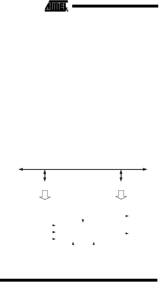
Figure 27 shows a block diagram of the Output Compare unit.
Figure 27. Output Compare Unit, Block Diagram
DATA BUS
|
OCRnx |
|
|
|
|
|
TCNTn |
|||||
|
|
|
|
|
|
|
|
|
|
|
|
|
|
|
|
|
|
|
|
|
|
|
|
|
|
|
|
|
= (8-bit Comparator ) |
|
|
|
|
|||||
|
|
|
|
|
|
|
|
|
OCFnx (Int.Req.) |
|||
top |
|
|
|
|
|
|
|
|
|
|
|
|
|
|
|
|
|
|
|
|
|
|
|
|
|
|
|
|
|
|
|
|
|
|
|
|
|
|
|
|
|
|
|
|
|
|
|
|
|
|
|
bottom |
|
|
Waveform Generator |
|
|
|
|
|||||
|
|
|
|
OCnx |
|
|||||||
FOCn |
|
|
|
|
|
|||||||
|
|
|
|
|
|
|
|
|
|
|
||
|
|
|
|
|
|
|
|
|
|
|
|
|
|
|
|
|
|
|
|
|
|
|
|
||
|
|
|
|
|
|
|
|
|
|
|||
|
|
|
|
|
|
|
|
|
|
|
||
|
|
|
WGMn1:0 |
COMnX1:0 |
|
|
|
|
||||
56 ATtiny13
2535A–AVR–06/03

|
|
|
ATtiny13 |
|
|
|
|
|
|
|
|
|
|
The OCR0x Registers are double buffered when using any of the Pulse Width Modula- |
|
|
|
tion (PWM) modes. For the normal and Clear Timer on Compare (CTC) modes of |
|
|
|
operation, the double buffering is disabled. The double buffering synchronizes the |
|
|
|
update of the OCR0x Compare Registers to either top or bottom of the counting |
|
|
|
sequence. The synchronization prevents the occurrence of odd-length, non-symmetrical |
|
|
|
PWM pulses, thereby making the output glitch-free. |
|
|
|
The OCR0x Register access may seem complex, but this is not case. When the double |
|
|
|
buffering is enabled, the CPU has access to the OCR0x Buffer Register, and if double |
|
|
|
buffering is disabled the CPU will access the OCR0x directly. |
|
Force Output Compare |
In non-PWM waveform generation modes, the match output of the comparator can be |
||
|
|
forced by writing a one to the Force Output Compare (FOC0x) bit. Forcing Compare |
|
|
|
Match will not set the OCF0x Flag or reload/clear the timer, but the OC0x pin will be |
|
|
|
updated as if a real Compare Match had occurred (the COM0x1:0 bits settings define |
|
|
|
whether the OC0x pin is set, cleared or toggled). |
|
Compare Match Blocking by |
All CPU write operations to the TCNT0 Register will block any Compare Match that |
||
TCNT0 Write |
occur in the next timer clock cycle, even when the timer is stopped. This feature allows |
||
|
|
OCR0x to be initialized to the same value as TCNT0 without triggering an interrupt when |
|
|
|
the Timer/Counter clock is enabled. |
|
Using the Output Compare |
Since writing TCNT0 in any mode of operation will block all Compare Matches for one |
||
Unit |
timer clock cycle, there are risks involved when changing TCNT0 when using the Output |
||
|
|
Compare Unit, independently of whether the Timer/Counter is running or not. If the |
|
|
|
value written to TCNT0 equals the OCR0x value, the Compare Match will be missed, |
|
|
|
resulting in incorrect waveform generation. Similarly, do not write the TCNT0 value |
|
|
|
equal to BOTTOM when the counter is down-counting. |
|
|
|
The setup of the OC0x should be performed before setting the Data Direction Register |
|
|
|
for the port pin to output. The easiest way of setting the OC0x value is to use the Force |
|
|
|
Output Compare (FOC0x) strobe bits in Normal mode. The OC0x Registers keep their |
|
|
|
values even when changing between Waveform Generation modes. |
|
|
|
Be aware that the COM0x1:0 bits are not double buffered together with the compare |
|
|
|
value. Changing the COM0x1:0 bits will take effect immediately. |
|
57
2535A–AVR–06/03

Compare Match Output
Unit
The Compare Output mode (COM0x1:0) bits have two functions. The Waveform Generator uses the COM0x1:0 bits for defining the Output Compare (OC0x) state at the next Compare Match. Also, the COM0x1:0 bits control the OC0x pin output source. Figure 28 shows a simplified schematic of the logic affected by the COM0x1:0 bit setting. The I/O Registers, I/O bits, and I/O pins in the figure are shown in bold. Only the parts of the general I/O Port Control Registers (DDR and PORT) that are affected by the COM0x1:0 bits are shown. When referring to the OC0x state, the reference is for the internal OC0x Register, not the OC0x pin. If a system reset occur, the OC0x Register is reset to “0”.
Figure 28. Compare Match Output Unit, Schematic
COMnx1 |
|
|
|
|
|
|
|
|
|
|
|
|
|
|
|
|
|
|
|
|
|
|
|
|
|
|
|
|
|
|
|
|
|
|
|
|
|
|
|
|
|
||
|
|
|
|
|
|
|
|
|
|
|
|
|
|
|
|
|
|
|
|
||
|
|
|
|
|
|
|
|
|
|
|
|
|
|
|
|
|
|
|
|
||
|
|
|
|
|
|
|
|
|
|
|
|
|
|
|
|
|
|
|
|
||
|
Waveform |
|
|
|
|
|
|
|
|
|
|
|
|
||||||||
|
|
|
|
|
|
|
|
|
|
|
|
|
|
|
|
|
|||||
COMnx0 |
|
|
|
|
D |
Q |
|
|
|
|
|
|
|
||||||||
|
|
|
|
|
Generator |
|
|
|
|
|
|
|
|
|
|
||||||
FOCn |
|
|
|
|
|
|
|
|
|
|
|
||||||||||
|
|
|
|
|
|
|
|
|
|
|
|
|
|||||||||
|
|
|
|
|
|
|
|
|
|
|
|
|
|
|
|
|
|
|
|
|
|
|
|
|
|
|
|
|
|
|
|
|
|
|
|
|
1 |
|
|
|
|
|
|
|
|
|
|
|
|
|
|
|
|
|
|
|
|
|
|
|
|
|
|
|
OCn |
|
|
|
|
|
|
|
|
|
|
|
|
|
OCnx |
0 |
|
|
|
|
Pin |
||
|
|
|
|
|
|
|
|
|
|
|
|
|
|
|
|
|
|||||
|
|
|
|
|
|
|
|
|
|
|
|
|
|
|
|
|
|
|
|
||
|
|
|
|
|
|
|
|
|
|
|
|
|
|
|
|
|
|
|
|
|
|
|
|
|
|
|
|
|
|
BUS |
|
|
|
|
D |
Q |
|
|
|
|
|
|
|
|
|
|
|
|
|
|
|
|
|
|
|
|
|
|
|
|
|
|
|||
|
|
|
|
|
|
|
|
|
|
|
|
|
|
|
|
|
|
|
|||
|
|
|
|
|
|
|
|
|
|
|
|
|
|
|
|
|
|
|
|
||
|
|
|
|
PORT |
|
|
|
|
|
|
|
||||||||||
|
|
|
|
|
|
|
|
DATA |
|
|
|
|
|
|
|
|
|
|
|
|
|
|
|
|
|
D |
Q |
|
|
|
|
|
|
|
|||||||||
|
|
|
|
|
|
|
|
|
|
|
|
|
|
|
|
|
|
|
|
||
|
|
|
|
|
|
|
|
|
|
|
|
|
|
|
|
|
|
|
|
|
|
|
|
|
|
|
|
|
|
|
|
|
|
|
|
|
|
|
|
|
|
|
|
|
clkI/O |
|
|
|
|
|
|
|
|
|
DDR |
|
|
|
|
|
|
|
|||
|
|
|
|
|
|
|
|
|
|
|
|
|
|
|
|
|
|
|
|||
The general I/O port function is overridden by the Output Compare (OC0x) from the Waveform Generator if either of the COM0x1:0 bits are set. However, the OC0x pin direction (input or output) is still controlled by the Data Direction Register (DDR) for the port pin. The Data Direction Register bit for the OC0x pin (DDR_OC0x) must be set as output before the OC0x value is visible on the pin. The port override function is independent of the Waveform Generation mode.
The design of the Output Compare pin logic allows initialization of the OC0x state before the output is enabled. Note that some COM0x1:0 bit settings are reserved for certain modes of operation. See “8-bit Timer/Counter Register Description” on page 65.
Compare Output Mode and The Waveform Generator uses the COM0x1:0 bits differently in Normal, CTC, and PWM Waveform Generation modes. For all modes, setting the COM0x1:0 = 0 tells the Waveform Generator that no action on the OC0x Register is to be performed on the next Compare Match. For compare output actions in the non-PWM modes refer to Table 27 on page 65. For fast PWM mode, refer to Table 28 on page 65, and for phase correct PWM refer to Table 29 on
page 66.
A change of the COM0x1:0 bits state will have effect at the first Compare Match after the bits are written. For non-PWM modes, the action can be forced to have immediate effect by using the FOC0x strobe bits.
58 ATtiny13
2535A–AVR–06/03