


Software Break Points
Limitations of debugWIRE
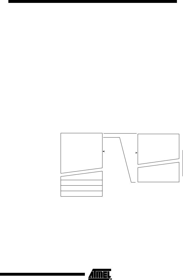
debugWIRE Related Register in I/O Memory
debugWire Data Register – DWDR
ATtiny13
•Capacitors inserted on the RESET pin must be disconnected when using debugWire.
•All external reset sources must be disconnected.
debugWIRE supports Program memory Break Points by the AVR Break instruction. Setting a Break Point in AVR Studio® will insert a BREAK instruction in the Program memory. The instruction replaced by the BREAK instruction will be stored. When program execution is continued, the stored instruction will be executed before continuing from the Program memory. A break can be inserted manually by putting the BREAK instruction in the program.
The Flash must be re-programmed each time a Break Point is changed. This is automatically handled by AVR Studio through the debugWIRE interface. The use of Break Points will therefore reduce the Falsh Data retention. Devices used for debugging purposes should not be shipped to end customers.
The debugWIRE communication pin (dW) is physically located on the same pin as External Reset (RESET). An External Reset source is therefore not supported when the debugWIRE is enabled.
The debugWIRE system accurately emulates all I/O functions when running at full speed, i.e., when the program in the CPU is running. When the CPU is stopped, care must be taken while accessing some of the I/O Registers via the debugger (AVR Studio). See the debugWIRE documentation for detailed description of the limitations.
A programmed DWEN Fuse enables some parts of the clock system to be running in all sleep modes. This will increase the power consumption while in sleep. Thus, the DWEN Fuse should be disabled when debugWire is not used.
The following section describes the registers used with the debugWire.
Bit |
7 |
6 |
5 |
4 |
3 |
2 |
1 |
0 |
|
|
|
|
|
DWDR[7:0] |
|
|
|
DWDR |
|
|
|
|
|
|
|
|
|
|
|
Read/Write |
R/W |
R/W |
R/W |
R/W |
R/W |
R/W |
R/W |
R/W |
|
Initial Value |
0 |
0 |
0 |
0 |
0 |
0 |
0 |
0 |
|
The DWDR Register provides a communication channel from the running program in the MCU to the debugger. This register is only accessible by the debugWIRE and can therefore not be used as a general purpose register in the normal operations.
93
2535A–AVR–06/03

Self-Programming
the Flash
The device provides a Self-Programming mechanism for downloading and uploading program code by the MCU itself. The Self-Programming can use any available data interface and associated protocol to read code and write (program) that code into the Program memory.
The Program memory is updated in a page by page fashion. Before programming a page with the data stored in the temporary page buffer, the page must be erased. The temporary page buffer is filled one word at a time using SPM and the buffer can be filled either before the Page Erase command or between a Page Erase and a Page Write operation:
Alternative 1, fill the buffer before a Page Erase
•Fill temporary page buffer
•Perform a Page Erase
•Perform a Page Write
Alternative 2, fill the buffer after Page Erase
•Perform a Page Erase
•Fill temporary page buffer
•Perform a Page Write
|
If only a part of the page needs to be changed, the rest of the page must be stored (for |
|
example in the temporary page buffer) before the erase, and then be re-written. When |
|
using alternative 1, the Boot Loader provides an effective Read-Modify-Write feature |
|
which allows the user software to first read the page, do the necessary changes, and |
|
then write back the modified data. If alternative 2 is used, it is not possible to read the |
|
old data while loading since the page is already erased. The temporary page buffer can |
|
be accessed in a random sequence. It is essential that the page address used in both |
|
the Page Erase and Page Write operation is addressing the same page. |
Performing Page Erase by |
To execute Page Erase, set up the address in the Z-pointer, write “00000011” to |
SPM |
SPMCSR and execute SPM within four clock cycles after writing SPMCSR. The data in |
|
R1 and R0 is ignored. The page address must be written to PCPAGE in the Z-register. |
|
Other bits in the Z-pointer will be ignored during this operation. |
|
• The CPU is halted during the Page Erase operation. |
Filling the Temporary Buffer |
To write an instruction word, set up the address in the Z-pointer and data in R1:R0, write |
(Page Loading) |
“00000001” to SPMCSR and execute SPM within four clock cycles after writing |
|
SPMCSR. The content of PCWORD in the Z-register is used to address the data in the |
|
temporary buffer. The temporary buffer will auto-erase after a Page Write operation or |
|
by writing the CTPB bit in SPMCSR. It is also erased after a system reset. Note that it is |
|
not possible to write more than one time to each address without erasing the temporary |
|
buffer. |
|
If the EEPROM is written in the middle of an SPM Page Load operation, all data loaded |
|
will be lost. |
Performing a Page Write |
To execute Page Write, set up the address in the Z-pointer, write “00000101” to |
|
SPMCSR and execute SPM within four clock cycles after writing SPMCSR. The data in |
|
R1 and R0 is ignored. The page address must be written to PCPAGE. Other bits in the |
|
Z-pointer must be written to zero during this operation. |
|
• The CPU is halted during the Page Write operation. |
94 ATtiny13
2535A–AVR–06/03
Addressing the Flash
During Self-
Programming
ATtiny13
The Z-pointer is used to address the SPM commands.
Bit |
15 |
14 |
13 |
12 |
11 |
10 |
9 |
8 |
ZH (R31) |
Z15 |
Z14 |
Z13 |
Z12 |
Z11 |
Z10 |
Z9 |
Z8 |
ZL (R30) |
|
|
|
|
|
|
|
|
Z7 |
Z6 |
Z5 |
Z4 |
Z3 |
Z2 |
Z1 |
Z0 |
|
|
|
|
|
|
|
|
|
|
|
7 |
6 |
5 |
4 |
3 |
2 |
1 |
0 |
Since the Flash is organized in pages (see Table 47 on page 101), the Program Counter can be treated as having two different sections. One section, consisting of the least significant bits, is addressing the words within a page, while the most significant bits are addressing the pages. This is shown in Figure 52. Note that the Page Erase and Page Write operations are addressed independently. Therefore it is of major importance that the software addresses the same page in both the Page Erase and Page Write operation.
The LPM instruction uses the Z-pointer to store the address. Since this instruction addresses the Flash byte-by-byte, also the LSB (bit Z0) of the Z-pointer is used.
Figure 52. Addressing the Flash During SPM(1)
BIT 15 |
|
|
|
ZPCMSB |
|
|
|
ZPAGEMSB 1 0 |
|
|||||||||
Z - REGISTER |
|
|
|
|
|
|
|
|
|
|
|
|
0 |
|
|
|
|
|
|
|
|
|
|
|
|
|
|
|
|
|
|
|
|
|
|
|
|
|
PROGRAM |
|
PCMSB |
|
|
|
PAGEMSB |
|
|
|
|
|||||||
|
|
|
PCPAGE |
PCWORD |
|
|
|
|
|
|||||||||
|
COUNTER |
|
|
|
|
|
||||||||||||
|
|
|
|
|
|
|
|
|
|
|
|
|
|
|||||
|
|
|
PAGE ADDRESS |
|
|
WORD ADDRESS |
|
|||||||||||
|
|
|
WITHIN THE FLASH |
|
|
WITHIN A PAGE |
|
|||||||||||
PROGRAM MEMORY |
|
|
|
|
|
|
|
|
|
PAGE |
PCWORD[PAGEMSB:0]: |
|||||||
|
|
|
|
|
|
|
|
|
|
|
|
|
|
|
|
|
|
|
|
PAGE |
|
|
|
|
|
|
|
|
|
|
|
|
INSTRUCTION WORD |
00 |
|||
|
|
|
|
|
|
|
|
|
|
|
|
|
|
|
||||
|
|
|
|
|
|
|
|
|
|
|
|
|
|
|
|
|
|
01 |
|
|
|
|
|
|
|
|
|
|
|
|
|
|
|
|
|
|
|
|
|
|
|
|
|
|
|
|
|
|
|
|
|
|
|
|
|
02 |
|
|
|
|
|
|
|
|
|
|
|
|
|
|
|
|
|
|
|
|
|
|
|
|
|
|
|
|
|
|
|
|
|
|
|
|
|
|
|
|
|
|
|
|
|
|
|
|
|
|
|
|
|
|
|
|
|
|
|
|
|
|
|
|
|
|
|
|
|
|
|
|
|
|
|
|
|
|
|
|
|
|
|
|
|
|
|
|
|
|
|
|
|
|
|
|
|
|
|
|
|
|
|
|
|
|
|
|
|
|
|
|
|
|
|
|
|
|
|
|
|
|
|
|
|
|
|
|
|
|
|
|
|
|
|
|
|
|
|
|
|
|
|
|
|
|
|
|
|
|
|
|
|
|
|
|
|
|
|
|
|
|
|
|
|
|
|
|
|
|
|
|
|
|
|
|
|
|
|
|
|
|
|
|
|
|
|
|
|
|
|
|
|
|
|
|
|
|
|
|
|
|
|
|
|
|
|
|
|
|
|
|
|
|
|
|
|
|
|
|
|
|
|
|
|
|
|
|
|
|
|
|
|
|
|
|
|
|
|
|
|
|
|
|
|
|
|
|
|
|
|
|
|
|
|
|
|
|
|
|
|
|
|
|
|
|
PAGEEND
Note: 1. The different variables used in Figure 52 are listed in Table 47 on page 101.
95
2535A–AVR–06/03

Store Program Memory
Control and Status Register –
SPMCSR
The Store Program Memory Control and Status Register contains the control bits needed to control the Program memory operations.
Bit |
7 |
6 |
5 |
4 |
3 |
2 |
1 |
0 |
|
|
– |
– |
– |
CTPB |
RFLB |
PGWRT |
PGERS |
SPMEN |
SPMCSR |
|
|
|
|
|
|
|
|
|
|
Read/Write |
R |
R |
R |
R/W |
R/W |
R/W |
R/W |
R/W |
|
Initial Value |
0 |
0 |
0 |
0 |
0 |
0 |
0 |
0 |
|
• Bits 7..5 – Res: Reserved Bits
These bits are reserved bits in the ATtiny13 and always read as zero.
• Bit 4 – CTPB: Clear Temporary Page Buffer
If the CTPB bit is written while filling the temporary page buffer, the temporary page buffer will be cleared and the data will be lost.
• Bit 3 – RFLB: Read Fuse and Lock Bits
An LPM instruction within three cycles after RFLB and SPMEN are set in the SPMCSR Register, will read either the Lock bits or the Fuse bits (depending on Z0 in the Z- pointer) into the destination register. See “EEPROM Write Prevents Writing to SPMCSR” on page 97 for details.
• Bit 2 – PGWRT: Page Write
If this bit is written to one at the same time as SPMEN, the next SPM instruction within four clock cycles executes Page Write, with the data stored in the temporary buffer. The page address is taken from the high part of the Z-pointer. The data in R1 and R0 are ignored. The PGWRT bit will auto-clear upon completion of a Page Write, or if no SPM instruction is executed within four clock cycles. The CPU is halted during the entire Page Write operation.
• Bit 1 – PGERS: Page Erase
If this bit is written to one at the same time as SPMEN, the next SPM instruction within four clock cycles executes Page Erase. The page address is taken from the high part of the Z-pointer. The data in R1 and R0 are ignored. The PGERS bit will auto-clear upon completion of a Page Erase, or if no SPM instruction is executed within four clock cycles. The CPU is halted during the entire Page Write operation.
• Bit 0 – SPMEN: Store Program Memory Enable
This bit enables the SPM instruction for the next four clock cycles. If written to one together with either CTPB, RFLB, PGWRT, or PGERS, the following SPM instruction will have a special meaning, see description above. If only SPMEN is written, the following SPM instruction will store the value in R1:R0 in the temporary page buffer addressed by the Z-pointer. The LSB of the Z-pointer is ignored. The SPMEN bit will auto-clear upon completion of an SPM instruction, or if no SPM instruction is executed within four clock cycles. During Page Erase and Page Write, the SPMEN bit remains high until the operation is completed.
Writing any other combination than “10001”, “01001”, “00101”, “00011” or “00001” in the lower five bits will have no effect.
96 ATtiny13
2535A–AVR–06/03