


|
|
|
ATtiny13 |
|
|
|
|
ADC Voltage Reference |
|
||
The reference voltage for the ADC (VREF) indicates the conversion range for the ADC. |
|||
|
|
Single ended channels that exceed VREF will result in codes close to 0x3FF. VREF can be |
|
|
|
selected as either VCC, or internal 1.1V reference, or external AREF pin. The first ADC |
|
|
|
conversion result after switching reference voltage source may be inaccurate, and the |
|
|
|
user is advised to discard this result. |
|
ADC Noise Canceler The ADC features a noise canceler that enables conversion during sleep mode to reduce noise induced from the CPU core and other I/O peripherals. The noise canceler can be used with ADC Noise Reduction and Idle mode. To make use of this feature, the following procedure should be used:
1.Make sure that the ADC is enabled and is not busy converting. Single Conversion mode must be selected and the ADC conversion complete interrupt must be enabled.
2.Enter ADC Noise Reduction mode (or Idle mode). The ADC will start a conversion once the CPU has been halted.
3.If no other interrupts occur before the ADC conversion completes, the ADC interrupt will wake up the CPU and execute the ADC Conversion Complete interrupt routine. If another interrupt wakes up the CPU before the ADC conversion is complete, that interrupt will be executed, and an ADC Conversion Complete interrupt request will be generated when the ADC conversion completes. The CPU will remain in active mode until a new sleep command is executed.
Note that the ADC will not be automatically turned off when entering other sleep modes than Idle mode and ADC Noise Reduction mode. The user is advised to write zero to ADEN before entering such sleep modes to avoid excessive power consumption.
83
2535A–AVR–06/03
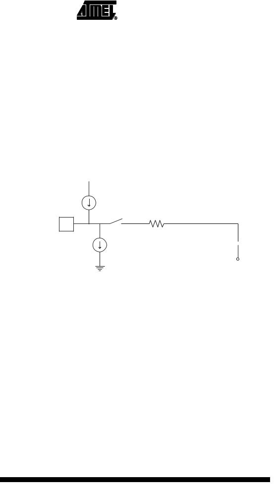
Analog Input Circuitry |
|
|
|
|
|
|
|
|
|
|
|
|
|
|
|
The analog input circuitry for single ended channels is illustrated in Figure 46. An analog |
|||||||
|
source applied to ADCn is subjected to the pin capacitance and input leakage of that |
||||||
|
pin, regardless of whether that channel is selected as input for the ADC. When the chan- |
||||||
|
nel is selected, the source must drive the S/H capacitor through the series resistance |
||||||
|
(combined resistance in the input path). |
||||||
|
The ADC is optimized for analog signals with an output impedance of approximately |
||||||
|
10 kΩ or less. If such a source is used, the sampling time will be negligible. If a source |
||||||
|
with higher impedance is used, the sampling time will depend on how long time the |
||||||
|
source needs to charge the S/H capacitor, with can vary widely. The user is recom- |
||||||
|
mended to only use low impedant sources with slowly varying signals, since this |
||||||
|
minimizes the required charge transfer to the S/H capacitor. |
||||||
|
Signal components higher than the Nyquist frequency (fADC/2) should not be present to |
||||||
|
avoid distortion from unpredictable signal convolution. The user is advised to remove |
||||||
|
high frequency components with a low-pass filter before applying the signals as inputs |
||||||
|
to the ADC. |
||||||
|
Figure 46. Analog Input Circuitry |
||||||
|
|
|
|
|
|
|
|
IIH
ADCn
1..100 kΩ
CS/H= 14 pF 
IIL
VCC/2
84 ATtiny13
2535A–AVR–06/03
 ATtiny13
Analog Noise Canceling
Techniques
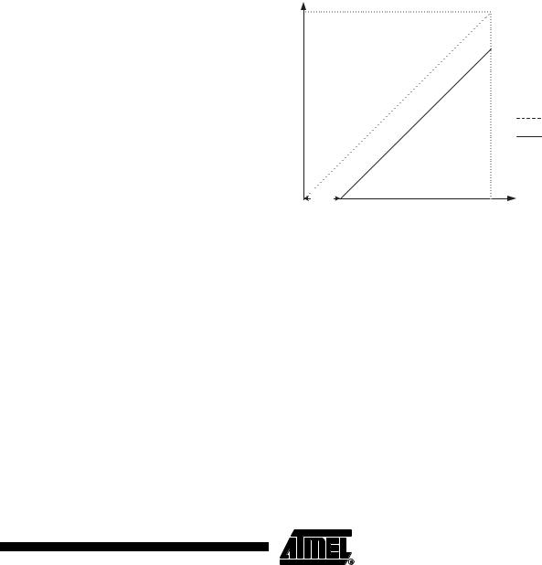
ADC Accuracy Definitions
Digital circuitry inside and outside the device generates EMI which might affect the accuracy of analog measurements. If conversion accuracy is critical, the noise level can be reduced by applying the following techniques:
1.Keep analog signal paths as short as possible. Make sure analog tracks run over the analog ground plane, and keep them well away from high-speed switching digital tracks.
2.Use the ADC noise canceler function to reduce induced noise from the CPU.
3.If any port pins are used as digital outputs, it is essential that these do not switch while a conversion is in progress.
An n-bit single-ended ADC converts a voltage linearly between GND and VREF in 2n steps (LSBs). The lowest code is read as 0, and the highest code is read as 2n-1.
Several parameters describe the deviation from the ideal behavior:
• Offset: The deviation of the first transition (0x000 to 0x001) compared to the ideal transition (at 0.5 LSB). Ideal value: 0 LSB.
Figure 47. |
Offset Error |
|
|
|
Output Code |
|
|
|
|
|
Ideal ADC |
|
|
|
Actual ADC |
|
Offset |
|
|
|
Error |
VREF |
Input Voltage |
|
|
• Gain Error: After adjusting for offset, the Gain Error is found as the deviation of the last transition (0x3FE to 0x3FF) compared to the ideal transition (at 1.5 LSB below maximum). Ideal value: 0 LSB
85
2535A–AVR–06/03
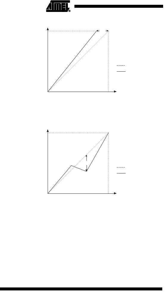
Figure 48. Gain Error
Output Code |
Gain |
|
|
Error |
|
|
|
Ideal ADC |
|
|
Actual ADC |
|
VREF |
Input Voltage |
• Integral Non-linearity (INL): After adjusting for offset and gain error, the INL is the maximum deviation of an actual transition compared to an ideal transition for any code. Ideal value: 0 LSB.
Figure 49. Integral Non-linearity (INL) |
|
Output Code |
|
INL |
Ideal ADC |
|
|
|
Actual ADC |
VREF |
Input Voltage |
• Differential Non-linearity (DNL): The maximum deviation of the actual code width (the interval between two adjacent transitions) from the ideal code width (1 LSB). Ideal value: 0 LSB.
86 ATtiny13
2535A–AVR–06/03

ATtiny13
Figure 50. Differential Non-linearity (DNL)
Output Code
0x3FF
|
1 LSB |
|
DNL |
0x000 |
|
0 |
VREF Input Voltage |
•Quantization Error: Due to the quantization of the input voltage into a finite number of codes, a range of input voltages (1 LSB wide) will code to the same value. Always
± 0.5 LSB.
•Absolute Accuracy: The maximum deviation of an actual (unadjusted) transition compared to an ideal transition for any code. This is the compound effect of offset, gain error, differential error, non-linearity, and quantization error. Ideal value: ± 0.5 LSB.
87
2535A–AVR–06/03