


High-voltage Serial |
|
|
|
|
|
|
|
|
|
|
|
|
|
To program and verify the ATtiny13 in the High-voltage Serial Programming mode, the |
||||||
Programming Algorithm |
following sequence is recommended (See instruction formats in Table 56): |
|||||
Enter High-voltage Serial |
The following algorithm puts the device in High-voltage Serial Programming mode: |
|||||
Programming Mode |
1. |
Apply 4.5 - 5.5V between VCC and GND. |
||||
|
||||||
|
2. |
Set RESET pin to “0” and toggle SCI at least six times. |
||||
|
3. |
Set the Prog_enable pins listed in Table 54 to “000” and wait at least 100 ns. |
||||
|
4. |
Apply VHVRST - 5.5V to RESET. Keep the Prog_enable pins unchanged for at |
||||
|
|
least tHVRST after the High-voltage has been applied to ensure the Prog_enable |
||||
|
|
signature has been latched. |
||||
|
5. |
Shortly after latching the Prog_enable signature, the device will activly output |
||||
|
|
data on the Prog_enable[2]/SDO pin, and the resulting drive contention may |
||||
|
|
increase the power consumption. To minimize this drive contention, release the |
||||
|
|
Prog_enable[2] pin after tHVRST has elapsed. |
||||
|
6. |
Wait at least 50 µs before giving any serial instructions on SDI/SII. |
||||
Table 55. High-voltage Reset Characteristics
|
|
|
Minimum High-voltage Period |
|
Supply Voltage |
RESET Pin High-voltage Threshold |
for Latching Prog_enable |
|
|
|
|
|
VCC |
VHVRST |
tHVRST |
|
4.5V |
11.5V |
100 ns |
|
|
|
|
|
5.5V |
11.5V |
100 ns |
Considerations for Efficient |
|
|
|
The loaded command and address are retained in the device during programming. For |
|||
Programming |
efficient programming, the following should be considered. |
||
•The command needs only be loaded once when writing or reading multiple memory locations.
•Skip writing the data value 0xFF that is the contents of the entire EEPROM (unless the EESAVE Fuse is programmed) and Flash after a Chip Erase.
•Address High byte needs only be loaded before programming or reading a new 256 word window in Flash or 256 byte EEPROM. This consideration also applies to Signature bytes reading.
Chip Erase |
The Chip Erase will erase the Flash and EEPROM(1) memories plus Lock bits. The Lock |
|
|
bits are not reset until the Program memory has been completely erased. The Fuse bits |
|
|
are not changed. A Chip Erase must be performed before the Flash and/or EEPROM |
|
|
are re-programmed. |
|
|
Note: 1. The EEPROM memory is preserved during Chip Erase if the EESAVE Fuse is |
|
|
|
programmed. |
|
1. |
Load command “Chip Erase” (see Table 56). |
|
2. |
Wait after Instr. 3 until SDO goes high for the “Chip Erase” cycle to finish. |
|
3. |
Load Command “No Operation”. |
108 ATtiny13
2535A–AVR–06/03
|
|
|
|
ATtiny13 |
|
|
|
|
|
Programming the Flash |
|
|
||
The Flash is organized in pages, see Table 51 on page 105. When programming the |
||||
|
|
Flash, the program data is latched into a page buffer. This allows one page of program |
||
|
|
data to be programmed simultaneously. The following procedure describes how to pro- |
||
|
|
gram the entire Flash memory: |
||
|
|
1. |
Load Command “Write Flash” (see Table 56). |
|
|
|
2. |
Load Flash Page Buffer. |
|
|
|
3. |
Load Flash High Address and Program Page. Wait after Instr. 3 until SDO goes |
|
|
|
|
high for the “Page Programming” cycle to finish. |
|
|
|
4. |
Repeat 2 through 3 until the entire Flash is programmed or until all data has |
|
|
|
|
been programmed. |
|
|
|
5. |
End Page Programming by Loading Command “No Operation”. |
|
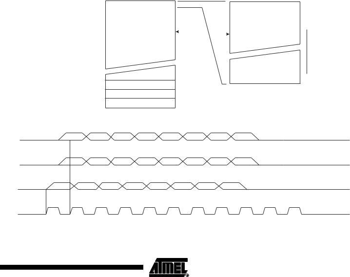
When writing or reading serial data to the ATtiny13, data is clocked on the rising edge of the serial clock, see Figure 58, Figure 59 and Table 57 for details.
Figure 57. Addressing the Flash which is Organized in Pages
|
PROGRAM |
PCMSB |
|
|
|
|
PAGEMSB |
|
|||||||
|
|
PCPAGE |
PCWORD |
|
|
|
|
||||||||
|
COUNTER |
|
|
|
|
|
|||||||||
|
|
|
|
|
|
|
|
|
|
|
|
|
|
||
|
PAGE ADDRESS |
|
|
WORD ADDRESS |
|
||||||||||
|
WITHIN THE FLASH |
|
|
WITHIN A PAGE |
|
||||||||||
PROGRAM MEMORY |
|
|
|
|
|
|
|
|
|
PAGE |
PCWORD[PAGEMSB:0]: |
||||
|
|
|
|
|
|
|
|
|
|
|
|
|
|
|
|
|
PAGE |
|
|
|
|
|
|
|
|
INSTRUCTION WORD |
00 |
||||
|
|
|
|
|
|
|
|
|
|
|
|
||||
|
|
|
|
|
|
|
|
|
|
|
|
|
|
|
01 |
|
|
|
|
|
|
|
|
|
|
|
|
|
|
|
|
|
|
|
|
|
|
|
|
|
|
|
|
|
|
|
02 |
|
|
|
|
|
|
|
|
|
|
|
|
|
|
|
|
|
|
|
|
|
|
|
|
|
|
|
|
|
|
|
|
|
|
|
|
|
|
|
|
|
|
|
|
|
|
|
|
|
|
|
|
|
|
|
|
|
|
|
|
|
|
|
|
|
|
|
|
|
|
|
|
|
|
|
|
|
|
|
|
|
|
|
|
|
|
|
|
|
|
|
|
|
|
|
|
|
|
|
|
|
|
|
|
|
|
|
|
|
|
|
|
|
|
|
|
|
|
|
|
|
|
|
|
|
|
|
|
|
|
|
|
|
|
|
|
|
|
|
|
|
|
|
|
|
|
|
|
|
|
|
|
|
|
|
|
|
|
|
|
|
|
|
|
|
|
|
|
|
|
|
|
|
|
|
|
|
|
|
|
|
|
|
|
|
|
|
|
|
|
|
|
|
|
|
|
|
|
|
|
|
|
|
|
|
|
|
|
|
|
|
|
|
|
|
|
|
|
|
|
|
|
|
|
PAGEEND
Figure 58. High-voltage Serial Programming Waveforms
SDI |
|
MSB |
|
|
|
|
|
|
LSB |
|
|
PB0 |
|
|
|
|
|
|
|
|
|
|
|
SII |
|
MSB |
|
|
|
|
|
|
LSB |
|
|
PB1 |
|
|
|
|
|
|
|
|
|
||
|
|
|
|
|
|
|
|
|
|
|
|
SDO |
|
MSB |
|
|
|
|
|
|
LSB |
|
|
PB2 |
|
|
|
|
|
|
|
|
|
|
|
SCI |
0 |
1 |
2 |
3 |
4 |
5 |
6 |
7 |
8 |
9 |
10 |
PB3 |
|
|
|
|
|
|
|
|
|
|
|
109
2535A–AVR–06/03

Programming the EEPROM |
|
|
|
|
|
|
|
|
|
|
|
|
|
The EEPROM is organized in pages, see Table 52 on page 106. When programming |
||||||
|
the EEPROM, the data is latched into a page buffer. This allows one page of data to be |
|||||
|
programmed simultaneously. The programming algorithm for the EEPROM Data mem- |
|||||
|
ory is as follows (refer to Table 56): |
|||||
|
1. |
Load Command “Write EEPROM”. |
||||
|
2. |
Load EEPROM Page Buffer. |
||||
|
3. |
Program EEPROM Page. Wait after Instr. 2 until SDO goes high for the “Page |
||||
|
|
Programming” cycle to finish. |
||||
|
4. |
Repeat 2 through 3 until the entire EEPROM is programmed or until all data has |
||||
|
|
been programmed. |
||||
|
5. |
End Page Programming by Loading Command “No Operation”. |
||||
Reading the Flash |
The algorithm for reading the Flash memory is as follows (refer to Table 56): |
|||||
|
1. |
Load Command "Read Flash". |
||||
|
2. |
Read Flash Low and High Bytes. The contents at the selected address are avail- |
||||
|
|
able at serial output SDO. |
||||
Reading the EEPROM |
The algorithm for reading the EEPROM memory is as follows (refer to Table 56): |
|||||
|
1. |
Load Command “Read EEPROM”. |
||||
|
2. |
Read EEPROM Byte. The contents at the selected address are available at |
||||
|
|
serial output SDO. |
||||
Programming and Reading |
The algorithms for programming and reading the Fuse Low/High bits and Lock bits are |
|||||
the Fuse and Lock Bits |
shown in Table 56. |
|||||
Reading the Signature Bytes |
The algorithms for reading the Signature bytes and Calibration byte are shown in Table |
|||||
and Calibration Byte |
56. |
|
|
|
|
|
Power-off sequence |
Set SCI to “0”. Set RESET to “1”. Turn V CC power off. |
|||||
110 ATtiny13
2535A–AVR–06/03
ATtiny13
Table 56. High-voltage Serial Programming Instruction Set for ATtiny13
|
|
|
Instruction Format |
|
|
||
|
|
|
|
|
|
|
|
Instruction |
|
Instr.1/5 |
Instr.2/6 |
Instr.3 |
Instr.4 |
Operation Remarks |
|
|
|
|
|
|
|
|
|
|
SDI |
0_1000_0000_00 |
0_0000_0000_00 |
0_0000_0000_00 |
|
Wait after Instr.3 until SDO goes |
|
Chip Erase |
SII |
0_0100_1100_00 |
0_0110_0100_00 |
0_0110_1100_00 |
|
high for the Chip Erase cycle to |
|
|
SDO |
x_xxxx_xxxx_xx |
x_xxxx_xxxx_xx |
x_xxxx_xxxx_xx |
|
finish. |
|
|
|
|
|
|
|
|
|
Load “Write |
SDI |
0_0001_0000_00 |
|
|
|
|
|
Flash” |
SII |
0_0100_1100_00 |
|
|
|
Enter Flash Programming code. |
|
Command |
SDO |
x_xxxx_xxxx_xx |
|
|
|
|
|
|
|
|
|
|
|
|
|
|
SDI |
0_ bbbb_bbbb _00 |
0_eeee_eeee_00 |
0_dddd_dddd_00 |
0_0000_0000_00 |
Repeat after Instr. 1 - 5 until the |
|
|
entire page buffer is filled or until all |
||||||
|
SII |
0_0000_1100_00 |
0_0010_1100_00 |
0_0011_1100_00 |
0_0111_1101_00 |
||
|
data within the page is filled. See |
||||||
|
SDO |
x_xxxx_xxxx_xx |
x_xxxx_xxxx_xx |
x_xxxx_xxxx_xx |
x_xxxx_xxxx_xx |
||
Load Flash |
Note 1. |
||||||
|
|
|
|
|
|||
Page Buffer |
|
|
|
|
|
|
|
SDI |
0_0000_0000_00 |
|
|
|
|
||
|
|
|
|
|
|||
|
SII |
0_0111_1100_00 |
|
|
|
Instr 5. |
|
|
SDO |
x_xxxx_xxxx_xx |
|
|
|
|
|
|
|
|
|
|
|
|
|
|
|
|
|
|
|
Wait after Instr 3 until SDO goes |
|
Load Flash High |
SDI |
0_0000_000a_00 |
0_0000_0000_00 |
0_0000_0000_00 |
|
high. Repeat Instr. 2 - 3 for each |
|
|
loaded Flash Page until the entire |
||||||
Address and |
SII |
0_0001_1100_00 |
0_0110_0100_00 |
0_0110_1100_00 |
|
||
|
Flash or all data is programmed. |
||||||
Program Page |
SDO |
x_xxxx_xxxx_xx |
x_xxxx_xxxx_xx |
x_xxxx_xxxx_xx |
|
||
|
Repeat Instr. 1 for a new 256 byte |
||||||
|
|
|
|
|
|
||
|
|
|
|
|
|
page. See Note 1. |
|
|
|
|
|
|
|
|
|
Load “Read |
SDI |
0_0000_0010_00 |
|
|
|
|
|
Flash” |
SII |
0_0100_1100_00 |
|
|
|
Enter Flash Read mode. |
|
Command |
SDO |
x_xxxx_xxxx_xx |
|
|
|
|
|
|
|
|
|
|
|
|
|
|
SDI |
0_bbbb_bbbb_00 |
0_0000_000a_00 |
0_0000_0000_00 |
0_0000_0000_00 |
Repeat Instr. 1, 3 - 6 for each new |
|
|
SII |
0_0000_1100_00 |
0_0001_1100_00 |
0_0110_1000_00 |
0_0110_1100_00 |
address. Repeat Instr. 2 for a new |
|
Read Flash Low |
SDO |
x_xxxx_xxxx_xx |
x_xxxx_xxxx_xx |
x_xxxx_xxxx_xx |
q_qqqq_qqqx_xx |
256 byte page. |
|
|
|||||||
and High Bytes |
SDI |
0_0000_0000_00 |
0_0000_0000_00 |
|
|
|
|
|
|
|
|
||||
|
SII |
0_0111_1000_00 |
0_0111_1100_00 |
|
|
Instr 5 - 6. |
|
|
SDO |
x_xxxx_xxxx_xx |
p_pppp_pppx_xx |
|
|
|
|
|
|
|
|
|
|
|
|
Load “Write |
SDI |
0_0001_0001_00 |
|
|
|
Enter EEPROM Programming |
|
EEPROM” |
SII |
0_0100_1100_00 |
|
|
|
||
|
|
|
mode. |
||||
Command |
SDO |
x_xxxx_xxxx_xx |
|
|
|
||
|
|
|
|
||||
|
|
|
|
|
|
|
|
|
SDI |
0_00bb_bbbb_00 |
0_eeee_eeee_00 |
0_0000_0000_00 |
0_0000_0000_00 |
Repeat Instr. 1 - 4 until the entire |
|
Load EEPROM |
page buffer is filled or until all data |
||||||
SII |
0_0000_1100_00 |
0_0010_1100_00 |
0_0110_1101_00 |
0_0110_1100_00 |
|||
Page Buffer |
within the page is filled. See Note |
||||||
SDO |
x_xxxx_xxxx_xx |
x_xxxx_xxxx_xx |
x_xxxx_xxxx_xx |
x_xxxx_xxxx_xx |
|||
|
2. |
||||||
|
|
|
|
|
|
||
|
|
|
|
|
|
|
|
|
SDI |
0_0000_0000_00 |
0_0000_0000_00 |
|
|
Wait after Instr. 2 until SDO goes |
|
Program |
|
|
high. Repeat Instr. 1 - 2 for each |
||||
SII |
0_0110_0100_00 |
0_0110_1100_00 |
|
|
loaded EEPROM page until the |
||
EEPROM Page |
|
|
|||||
SDO |
x_xxxx_xxxx_xx |
x_xxxx_xxxx_xx |
|
|
entire EEPROM or all data is |
||
|
|
|
|||||
|
|
|
|
|
|
programmed. |
|
|
|
|
|
|
|
|
|
|
SDI |
0_00bb_bbbb_00 |
0_eeee_eeee_00 |
0_0000_0000_00 |
0_0000_0000_00 |
Repeat Instr. 1 - 5 for each new |
|
|
SII |
0_0000_1100_00 |
0_0010_1100_00 |
0_0110_1101_00 |
0_0110_0100_00 |
address. Wait after Instr. 5 until |
|
Write EEPROM |
SDO |
x_xxxx_xxxx_xx |
x_xxxx_xxxx_xx |
x_xxxx_xxxx_xx |
x_xxxx_xxxx_xx |
SDO goes high. See Note 3. |
|
|
|
|
|
|
|
||
Byte |
SDI |
0_0000_0000_00 |
|
|
|
|
|
|
|
|
|
|
|||
|
SII |
0_0110_1100_00 |
|
|
|
Instr. 5 |
|
|
SDO |
x_xxxx_xxxx_xx |
|
|
|
|
|
|
|
|
|
|
|
|
|
111
2535A–AVR–06/03

Table 56. High-voltage Serial Programming Instruction Set for ATtiny13 (Continued)
|
|
|
Instruction Format |
|
|
||
|
|
|
|
|
|
|
|
Instruction |
|
Instr.1/5 |
Instr.2/6 |
Instr.3 |
Instr.4 |
Operation Remarks |
|
|
|
|
|
|
|
|
|
Load “Read |
SDI |
0_0000_0011_00 |
|
|
|
|
|
EEPROM” |
SII |
0_0100_1100_00 |
|
|
|
Enter EEPROM Read mode. |
|
Command |
SDO |
x_xxxx_xxxx_xx |
|
|
|
|
|
|
|
|
|
|
|
|
|
Read EEPROM |
SDI |
0_bbbb_bbbb_00 |
0_aaaa_aaaa_00 |
0_0000_0000_00 |
0_0000_0000_00 |
Repeat Instr. 1, 3 - 4 for each new |
|
SII |
0_0000_1100_00 |
0_0001_1100_00 |
0_0110_1000_00 |
0_0110_1100_00 |
address. Repeat Instr. 2 for a new |
||
Byte |
|||||||
SDO |
x_xxxx_xxxx_xx |
x_xxxx_xxxx_xx |
x_xxxx_xxxx_xx |
q_qqqq_qqq0_00 |
256 byte page. |
||
|
|||||||
|
|
|
|
|
|
|
|
Write Fuse Low |
SDI |
0_0100_0100_00 |
0_A987_6543_00 |
0_0000_0000_00 |
0_0000_0000_00 |
Wait after Instr. 4 until SDO goes |
|
SII |
0_0100_1100_00 |
0_0010_1100_00 |
0_0110_0100_00 |
0_0110_1100_00 |
high. Write A - 3 = “0” to program |
||
Bits |
|||||||
SDO |
x_xxxx_xxxx_xx |
x_xxxx_xxxx_xx |
x_xxxx_xxxx_xx |
x_xxxx_xxxx_xx |
the Fuse bit. |
||
|
|||||||
|
|
|
|
|
|
|
|
Write Fuse High |
SDI |
0_0100_0000_00 |
0_000F_EDCB_00 |
0_0000_0000_00 |
0_0000_0000_00 |
Wait after Instr. 4 until SDO goes |
|
SII |
0_0100_1100_00 |
0_0010_1100_00 |
0_0111_0100_00 |
0_0111_1100_00 |
high. Write F - B = “0” to program |
||
Bits |
SDO |
x_xxxx_xxxx_xx |
x_xxxx_xxxx_xx |
x_xxxx_xxxx_xx |
x_xxxx_xxxx_xx |
the Fuse bit. |
|
|
|||||||
|
|
|
|
|
|
|
|
|
SDI |
0_0010_0000_00 |
0_0000_0021_00 |
0_0000_0000_00 |
0_0000_0000_00 |
Wait after Instr. 4 until SDO goes |
|
Write Lock Bits |
SII |
0_0100_1100_00 |
0_0010_1100_00 |
0_0110_0100_00 |
0_0110_1100_00 |
high. Write 2 - 1 = “0” to program |
|
|
SDO |
x_xxxx_xxxx_xx |
x_xxxx_xxxx_xx |
x_xxxx_xxxx_xx |
x_xxxx_xxxx_xx |
the Lock Bit. |
|
|
|
|
|
|
|
|
|
Read Fuse Low |
SDI |
0_0000_0100_00 |
0_0000_0000_00 |
0_0000_0000_00 |
|
Reading A - 3 = “0” means the |
|
SII |
0_0100_1100_00 |
0_0110_1000_00 |
0_0110_1100_00 |
|
|||
Bits |
|
Fuse bit is programmed. |
|||||
SDO |
x_xxxx_xxxx_xx |
x_xxxx_xxxx_xx |
A_9876_543x_xx |
|
|||
|
|
|
|||||
|
|
|
|
|
|
|
|
Read Fuse High |
SDI |
0_0000_0100_00 |
0_0000_0000_00 |
0_0000_0000_00 |
|
Reading F - B = “0” means the |
|
SII |
0_0100_1100_00 |
0_0111_1010_00 |
0_0111_1110_00 |
|
|||
Bits |
SDO |
x_xxxx_xxxx_xx |
x_xxxx_xxxx_xx |
x_xxFE_DCBx_xx |
|
Fuse bit is programmed. |
|
|
|
|
|||||
|
|
|
|
|
|
|
|
|
SDI |
0_0000_0100_00 |
0_0000_0000_00 |
0_0000_0000_00 |
|
Reading 2, 1 = “0” means the Lock |
|
Read Lock Bits |
SII |
0_0100_1100_00 |
0_0111_1000_00 |
0_0111_1100_00 |
|
||
|
bit is programmed. |
||||||
|
SDO |
x_xxxx_xxxx_xx |
x_xxxx_xxxx_xx |
x_xxxx_x21x_xx |
|
||
|
|
|
|||||
|
|
|
|
|
|
|
|
Read Signature |
SDI |
0_0000_1000_00 |
0_0000_00bb_00 |
0_0000_0000_00 |
0_0000_0000_00 |
Repeats Instr 2 4 for each |
|
SII |
0_0100_1100_00 |
0_0000_1100_00 |
0_0110_1000_00 |
0_0110_1100_00 |
|||
Bytes |
signature byte address. |
||||||
SDO |
x_xxxx_xxxx_xx |
x_xxxx_xxxx_xx |
x_xxxx_xxxx_xx |
q_qqqq_qqqx_xx |
|||
|
|
||||||
|
|
|
|
|
|
|
|
Read |
SDI |
0_0000_1000_00 |
0_0000_0000_00 |
0_0000_0000_00 |
0_0000_0000_00 |
|
|
SII |
0_0100_1100_00 |
0_0000_1100_00 |
0_0111_1000_00 |
0_0111_1100_00 |
|
||
Calibration Byte |
|
||||||
|
SDO |
x_xxxx_xxxx_xx |
x_xxxx_xxxx_xx |
x_xxxx_xxxx_xx |
p_pppp_pppx_xx |
|
|
|
|
|
|
|
|
|
|
Load “No |
SDI |
0_0000_0000_00 |
|
|
|
|
|
Operation” |
SII |
0_0100_1100_00 |
|
|
|
|
|
Command |
SDO |
x_xxxx_xxxx_xx |
|
|
|
|
|
|
|
|
|
|
|
|
|
Note: a = address high bits, b = address low bits, d = data in high bits, e = data in low bits, p = data out high bits, q = data out low bits, x = don’t care, 1 = Lock Bit1, 2 = Lock Bit2, 3 = CKSEL0 Fuse, 4 = CKSEL1 Fuse, 5 = SUT0 Fuse, 6 = SUT1 Fuse, 7 = CKDIV8, Fuse, 8 = WDTON Fuse, 9 = EESAVE Fuse, A = SPIEN Fuse, B = RSTDISBL Fuse, C = BODLEVEL0 Fuse, D= BODLEVEL1 Fuse, E = MONEN Fuse, F = SPMEN Fuse
Notes: 1. For page sizes less than 256 words, parts of the address (bbbb_bbbb) will be parts of the page address.
2.For page sizes less than 256 bytes, parts of the address (bbbb_bbbb) will be parts of the page address.
3.The EEPROM is written page-wise. But only the bytes that are loaded into the page are actually written to the EEPROM. Page-wise EEPROM access is more efficient when multiple bytes are to be written to the same page. Note that auto-erase of EEPROM is not available in High-voltage Serial Programming, only in SPI Programming.
112 ATtiny13
2535A–AVR–06/03

High-voltage Serial
Programming
Characteristics
ATtiny13
Figure 59. High-voltage Serial Programming Timing
SDI (PB0), SII (PB1)
tIVSH |
|
|
|
tSHIX |
tSLSH |
|
|
SCI (PB3)
tSHSL
SDO (PB2)
tSHOV
Table 57. High-voltage Serial Programming Characteristics TA = 25°C ± 10%, VCC = 5.0V ± 10% (Unless otherwise noted)
Symbol |
Parameter |
Min |
Typ |
Max |
Units |
|
|
|
|
|
|
tSHSL |
SCI (PB3) Pulse Width High |
110 |
|
|
ns |
tSLSH |
SCI (PB3) Pulse Width Low |
110 |
|
|
ns |
tIVSH |
SDI (PB0), SII (PB1) Valid to SCI (PB3) High |
50 |
|
|
ns |
tSHIX |
SDI (PB0), SII (PB1) Hold after SCI (PB3) High |
50 |
|
|
ns |
tSHOV |
SCI (PB3) High to SDO (PB2) Valid |
|
16 |
|
ns |
tWLWH_PFB |
Wait after Instr. 3 for Write Fuse Bits |
|
2.5 |
|
ms |
113
2535A–AVR–06/03