


 ATtiny13
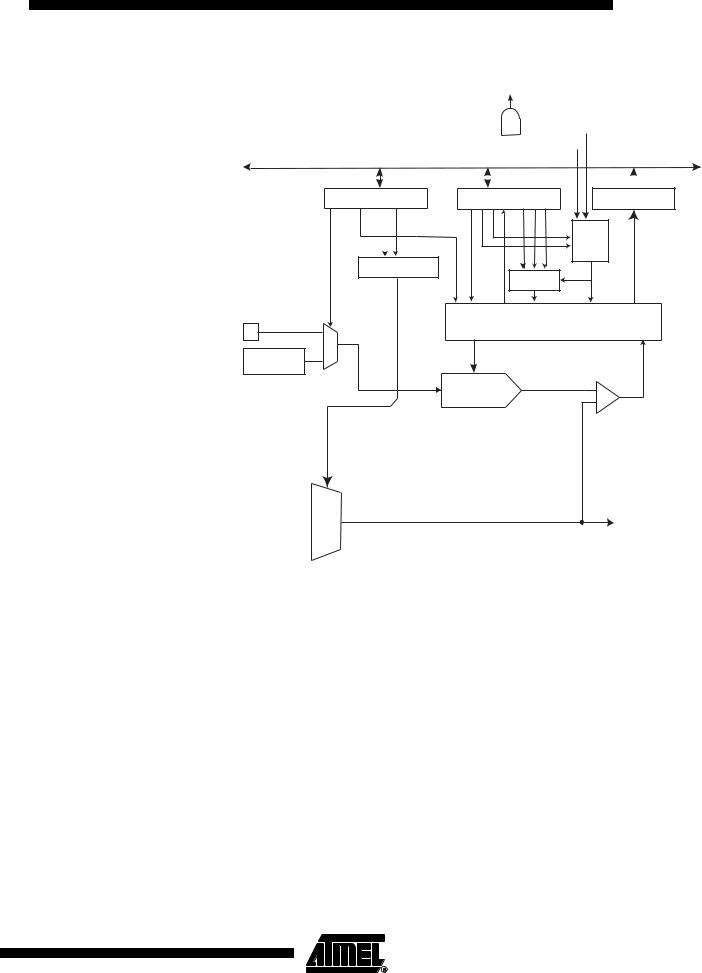
Analog Comparator
Multiplexed Input
Digital Input Disable Register
0 – DIDR0
It is possible to select any of the ADC3..0 pins to replace the negative input to the Analog Comparator. The ADC multiplexer is used to select this input, and consequently, the ADC must be switched off to utilize this feature. If the Analog Comparator Multiplexer Enable bit (ACME in ADCSRB) is set and the ADC is switched off (ADEN in ADCSRA is zero), MUX1..0 in ADMUX select the input pin to replace the negative input to the Analog Comparator, as shown in Table 36. If ACME is cleared or ADEN is set, AIN1 is applied to the negative input to the Analog Comparator.
Table 36. Analog Comparator Multiplexed Input
ACME |
ADEN |
MUX1..0 |
Analog Comparator Negative Input |
|
|
|
|
0 |
x |
xx |
AIN1 |
|
|
|
|
1 |
1 |
xx |
AIN1 |
|
|
|
|
1 |
0 |
00 |
ADC0 |
|
|
|
|
1 |
0 |
01 |
ADC1 |
|
|
|
|
1 |
0 |
10 |
ADC2 |
|
|
|
|
1 |
0 |
11 |
ADC3 |
|
|
|
|
Bit |
7 |
6 |
5 |
4 |
3 |
2 |
1 |
0 |
|
|
– |
– |
ADC0D |
ADC2D |
ADC3D |
ADC1D |
AIN1D |
AIN0D |
DIDR0 |
Read/Write |
R |
R |
R/W |
R/W |
R/W |
R/W |
R/W |
R/W |
|
Initial Value |
0 |
0 |
0 |
0 |
0 |
0 |
0 |
0 |
|
• Bits 1, 0 – AIN1D, AIN0D: AIN1, AIN0 Digital Input Disable
When this bit is written logic one, the digital input buffer on the AIN1/0 pin is disabled. The corresponding PIN Register bit will always read as zero when this bit is set. When an analog signal is applied to the AIN1/0 pin and the digital input from this pin is not needed, this bit should be written logic one to reduce power consumption in the digital input buffer.
75
2535A–AVR–06/03

Analog to Digital
Converter
Features |
• 10-bit Resolution |
|
• 0.5 LSB Integral Non-linearity |
|
• ± 2 LSB Absolute Accuracy |
|
• 13 - 260 µs Conversion Time |
|
• Up to 15 kSPS at Maximum Resolution |
|
• Four Multiplexed Single Ended Input Channels |
|
• Optional Left Adjustment for ADC Result Readout |
|
• 0 - VCC ADC Input Voltage Range |
|
• Selectable 1.1V ADC Reference Voltage |
|
• Free Running or Single Conversion Mode |
|
• ADC Start Conversion by Auto Triggering on Interrupt Sources |
|
• Interrupt on ADC Conversion Complete |
|
• Sleep Mode Noise Canceler |
|
The ATtiny13 features a 10-bit successive approximation ADC. The ADC is connected |
|
to a 4-channel Analog Multiplexer which allows four single-ended voltage inputs con- |
|
structed from the pins of Port B. The single-ended voltage inputs refer to 0V (GND). |
|
The ADC contains a Sample and Hold circuit which ensures that the input voltage to the |
|
ADC is held at a constant level during conversion. A block diagram of the ADC is shown |
|
in Figure 39. |
|
Internal reference voltages of nominally 1.1V or VCC are provided On-chip. |
76 ATtiny13
2535A–AVR–06/03
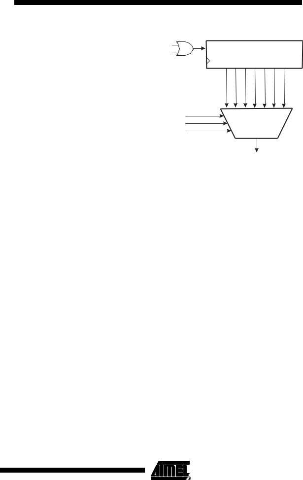
ATtiny13
Figure 39. Analog to Digital Converter Block Schematic
VCC
8-BIT DATA BUS
ADC MULTIPLEXER
SELECT (ADMUX)
REFS1 |
ADLAR |
MUX1 |
MUX0 |
|
|
|
|
MUX DECODER
CHANNEL SELECTION
INTERNAL 1.1V
REFERENCE
ADC CONVERSION
COMPLETE IRQ
INTERRUPT
FLAGS
|
|
|
|
ADTS[2:0] |
|
|
|
ADIF |
ADIE |
|
15 |
|
0 |
|
|
|
||||
|
||||||
ADC CTRL. & STATUS |
|
ADC DATA REGISTER |
||||
REGISTER (ADCSRA) |
|
(ADCH/ADCL) |
||||
ADEN |
ADSC |
ADATE |
ADIF |
ADPS2 |
ADPS1 |
ADPS0 |
TRIGGER |
ADC[9:0] |
|
|
|
|
|
|
|
SELECT |
|
PRESCALER
START
CONVERSION LOGIC
SAMPLE & HOLD
COMPARATOR
10-BIT DAC |
- |
+
ADC3 |
|
|
|
|
|
|
|
||
|
|
|
|
|
|
|
|
|
|
ADC2 |
|
|
INPUT |
ADC MULTIPLEXER |
|
|
|
||
|
|
|
MUX |
|
ADC1 |
|
|
OUTPUT |
|
|
|
|
||
|
|
|
|
|
|
|
|
|
|
|
|
|
|
|
ADC0 |
|
|
|
|
|
|
|
|
|
Operation |
The ADC converts an analog input voltage to a 10-bit digital value through successive |
|
approximation. The minimum value represents GND and the maximum value represents |
|
the voltage on VCC or an internal 1.1V reference voltage. |
|
The analog input channel is selected by writing to the MUX bits in ADMUX. Any of the |
|
ADC input pins, can be selected as single ended inputs to the ADC. |
|
The ADC is enabled by setting the ADC Enable bit, ADEN in ADCSRA. Voltage refer- |
|
ence and input channel selections will not go into effect until ADEN is set. The ADC |
|
does not consume power when ADEN is cleared, so it is recommended to switch off the |
|
ADC before entering power saving sleep modes. |
|
The ADC generates a 10-bit result which is presented in the ADC Data Registers, |
|
ADCH and ADCL. By default, the result is presented right adjusted, but can optionally |
|
be presented left adjusted by setting the ADLAR bit in ADMUX. |
|
If the result is left adjusted and no more than 8-bit precision is required, it is sufficient to |
|
read ADCH. Otherwise, ADCL must be read first, then ADCH, to ensure that the content |
|
of the data registers belongs to the same conversion. Once ADCL is read, ADC access |
|
to data registers is blocked. This means that if ADCL has been read, and a conversion |
|
completes before ADCH is read, neither register is updated and the result from the con- |
77
2535A–AVR–06/03

version is lost. When ADCH is read, ADC access to the ADCH and ADCL Registers is re-enabled.
The ADC has its own interrupt which can be triggered when a conversion completes.
When ADC access to the data registers is prohibited between reading of ADCH and
ADCL, the interrupt will trigger even if the result is lost.
Starting a Conversion A single conversion is started by writing a logical one to the ADC Start Conversion bit, ADSC. This bit stays high as long as the conversion is in progress and will be cleared by hardware when the conversion is completed. If a different data channel is selected while a conversion is in progress, the ADC will finish the current conversion before performing the channel change.
Alternatively, a conversion can be triggered automatically by various sources. Auto Triggering is enabled by setting the ADC Auto Trigger Enable bit, ADATE in ADCSRA. The trigger source is selected by setting the ADC Trigger Select bits, ADTS in ADCSRB (see description of the ADTS bits for a list of the trigger sources). When a positive edge occurs on the selected trigger signal, the ADC prescaler is reset and a conversion is started. This provides a method of starting conversions at fixed intervals. If the trigger signal still is set when the conversion completes, a new conversion will not be started. If another positive edge occurs on the trigger signal during conversion, the edge will be ignored. Note that an Interrupt Flag will be set even if the specific interrupt is disabled or the Global Interrupt Enable bit in SREG is cleared. A conversion can thus be triggered without causing an interrupt. However, the Interrupt Flag must be cleared in order to trigger a new conversion at the next interrupt event.
Figure 40. ADC Auto Trigger Logic
|
ADTS[2:0] |
PRESCALER |
|
|
|
|
START |
CLKADC |
ADIF |
ADATE |
|
SOURCE 1 |
|
|
. |
|
CONVERSION |
. |
|
|
|
LOGIC |
|
. |
|
|
|
|
|
. |
EDGE |
|
SOURCE n |
DETECTOR |
|
|
|
ADSC
Using the ADC Interrupt Flag as a trigger source makes the ADC start a new conversion as soon as the ongoing conversion has finished. The ADC then operates in Free Running mode, constantly sampling and updating the ADC Data Register. The first conversion must be started by writing a logical one to the ADSC bit in ADCSRA. In this mode the ADC will perform successive conversions independently of whether the ADC Interrupt Flag, ADIF is cleared or not.
If Auto Triggering is enabled, single conversions can be started by writing ADSC in ADCSRA to one. ADSC can also be used to determine if a conversion is in progress. The ADSC bit will be read as one during a conversion, independently of how the conversion was started.
78 ATtiny13
2535A–AVR–06/03
ATtiny13
Prescaling and |
Figure 41. ADC Prescaler |
|
Conversion Timing |
ADEN |
|
|
Reset |
|
|
START |
|
|
|
7-BIT ADC PRESCALER
CK 
CK/2 |
CK/4 |
CK/8 |
CK/16 |
CK/32 |
CK/64 |
CK/128 |
ADPS0
ADPS1
ADPS2
ADC CLOCK SOURCE
By default, the successive approximation circuitry requires an input clock frequency between 50 kHz and 200 kHz to get maximum resolution. If a lower resolution than 10 bits is needed, the input clock frequency to the ADC can be higher than 200 kHz to get a higher sample rate.
The ADC module contains a prescaler, which generates an acceptable ADC clock frequency from any CPU frequency above 100 kHz. The prescaling is set by the ADPS bits in ADCSRA. The prescaler starts counting from the moment the ADC is switched on by setting the ADEN bit in ADCSRA. The prescaler keeps running for as long as the ADEN bit is set, and is continuously reset when ADEN is low.
When initiating a single ended conversion by setting the ADSC bit in ADCSRA, the conversion starts at the following rising edge of the ADC clock cycle.
A normal conversion takes 13 ADC clock cycles. The first conversion after the ADC is switched on (ADEN in ADCSRA is set) takes 25 ADC clock cycles in order to initialize the analog circuitry.
The actual sample-and-hold takes place 1.5 ADC clock cycles after the start of a normal conversion and 14.5 ADC clock cycles after the start of an first conversion. When a conversion is complete, the result is written to the ADC Data Registers, and ADIF is set. In Single Conversion mode, ADSC is cleared simultaneously. The software may then set ADSC again, and a new conversion will be initiated on the first rising ADC clock edge.
When Auto Triggering is used, the prescaler is reset when the trigger event occurs. This assures a fixed delay from the trigger event to the start of conversion. In this mode, the sample-and-hold takes place two ADC clock cycles after the rising edge on the trigger source signal. Three additional CPU clock cycles are used for synchronization logic.
In Free Running mode, a new conversion will be started immediately after the conversion completes, while ADSC remains high. For a summary of conversion times, see Table 37.
79
2535A–AVR–06/03

Figure 42. ADC Timing Diagram, First Conversion (Single Conversion Mode)
|
|
|
|
|
|
|
First Conversion |
|
|
|
|
|
Next |
|
||
|
|
|
|
|
|
|
|
|
|
|
|
Conversion |
||||
|
|
|
|
|
|
|
|
|
|
|
|
|
|
|
||
Cycle Number |
1 |
2 |
12 |
13 |
14 15 |
16 |
17 |
18 |
19 20 |
21 |
22 |
23 |
24 |
25 |
1 2 |
3 |
ADC Clock |
|
|
|
|
|
|
|
|
|
|
|
|
|
|
|
|
ADEN |
|
|
|
|
|
|
|
|
|
|
|
|
|
|
|
|
ADSC |
|
|
|
|
|
|
|
|
|
|
|
|
|
|
|
|
ADIF |
|
|
|
|
|
|
|
|
|
|
|
|
|
|
|
|
ADCH |
|
|
|
|
|
|
|
|
|
|
|
|
|
Sign and MSB of Result |
||
|
|
|
|
|
|
|
|
|
|
|
|
|
|
|
|
|
ADCL |
|
|
|
|
|
|
|
|
|
|
|
|
|
|
LSB of Result |
|
|
|
|
|
|
|
|
|
|
|
|
|
|
|
|
|
|
|
|
MUX and REFS |
|
|
Sample & Hold |
|
|
Conversion |
|
|
|
MUX and REFS |
||||
|
|
Update |
|
|
|
|
|
Complete |
|
|
|
Update |
||||
|
|
|
|
|
|
|
|
|
|
|
|
|
||||
Figure 43. ADC Timing Diagram, Single Conversion |
|
|
|
|
|
|
||||||||||
|
|
|
|
|
|
|
One Conversion |
|
|
|
|
Next Conversion |
||||
Cycle Number |
|
1 2 |
3 |
4 |
5 |
6 |
7 |
8 |
9 |
10 |
11 |
12 |
13 |
1 |
2 |
3 |
ADC Clock |
|
|
|
|
|
|
|
|
|
|
|
|
|
|
|
|
ADSC |
|
|
|
|
|
|
|
|
|
|
|
|
|
|
|
|
ADIF |
|
|
|
|
|
|
|
|
|
|
|
|
|
|
|
|
ADCH |
|
|
|
|
|
|
|
|
|
|
|
|
|
Sign and MSB of Result |
||
ADCL |
|
|
|
|
|
|
|
|
|
|
|
|
|
LSB of Result |
||
|
|
|
|
Sample & Hold |
|
|
|
Conversion |
|
|
|
MUX and REFS |
||||
|
|
MUX and REFS |
|
|
|
|
|
|
|
|
||||||
|
|
|
|
|
|
|
Complete |
|
|
|
Update |
|||||
|
|
Update |
|
|
|
|
|
|
|
|
|
|
|
|
|
|
Figure 44. ADC Timing Diagram, Auto Triggered Conversion |
|
|
|
|
||||||||||||
|
|
|
|
|
|
|
|
One Conversion |
|
|
|
|
Next Conversion |
|||
Cycle Number |
|
1 |
2 |
3 |
4 |
5 |
6 |
7 |
8 |
9 |
10 |
11 |
12 |
13 |
|
1 2 |
ADC Clock |
|
|
|
|
|
|
|
|
|
|
|
|
|
|
|
|
Trigger |
|
|
|
|
|
|
|
|
|
|
|
|
|
|
|
|
Source |
|
|
|
|
|
|
|
|
|
|
|
|
|
|
|
|
ADATE |
|
|
|
|
|
|
|
|
|
|
|
|
|
|
|
|
ADIF |
|
|
|
|
|
|
|
|
|
|
|
|
|
|
|
|
ADCH |
|
|
|
|
|
|
|
|
|
|
|
|
|
Sign and MSB of Result |
||
ADCL |
|
|
|
|
|
|
|
|
|
|
|
|
|
|
LSB of Result |
|
Prescaler |
|
|
|
|
Sample & |
|
|
|
|
|
Conversion |
|
|
|
Prescaler |
|
|
|
|
|
Hold |
|
|
|
|
|
Complete |
|
|
|
Reset |
||
Reset |
|
|
|
|
|
|
|
|
|
|
|
|
||||
|
MUX and REFS |
|
|
|
|
|
|
|
|
|
|
|
|
|
||
|
|
|
|
|
|
|
|
|
|
|
|
|
|
|
||
|
|
Update |
|
|
|
|
|
|
|
|
|
|
|
|
|
|
80 ATtiny13
2535A–AVR–06/03
ATtiny13
Figure 45. ADC Timing Diagram, Free Running Conversion
|
One Conversion |
|
Next Conversion |
|
|||
Cycle Number |
11 |
12 |
13 |
1 |
2 |
3 |
4 |
|
|
|
|
|
|
|
|
ADC Clock |
|
|
|
|
|
|
|
ADSC |
|
|
|
|
|
|
|
ADIF |
|
|
|
|
|
|
|
ADCH |
|
|
|
Sign and MSB of Result |
|||
ADCL |
|
|
|
LSB of Result |
|
||
Conversion |
|
|
|
|
|
Sample & Hold |
|
|
|
|
|
|
|
||
Complete |
|
|
|
MUX and REFS |
|||
|
|
|
|
|
Update |
|
|
Table 37. ADC Conversion Time
|
Sample & Hold (Cycles |
Conversion Time |
Condition |
from Start of Conversion) |
(Cycles) |
|
|
|
First conversion |
14.5 |
25 |
|
|
|
Normal conversions |
1.5 |
13 |
|
|
|
Auto Triggered conversions |
2 |
13.5 |
|
|
|
81
2535A–AVR–06/03