

Analog Comparator
ADC Control and Status
Register B – ADCSRB
Analog Comparator Control
and Status Register – ACSR
ATtiny13
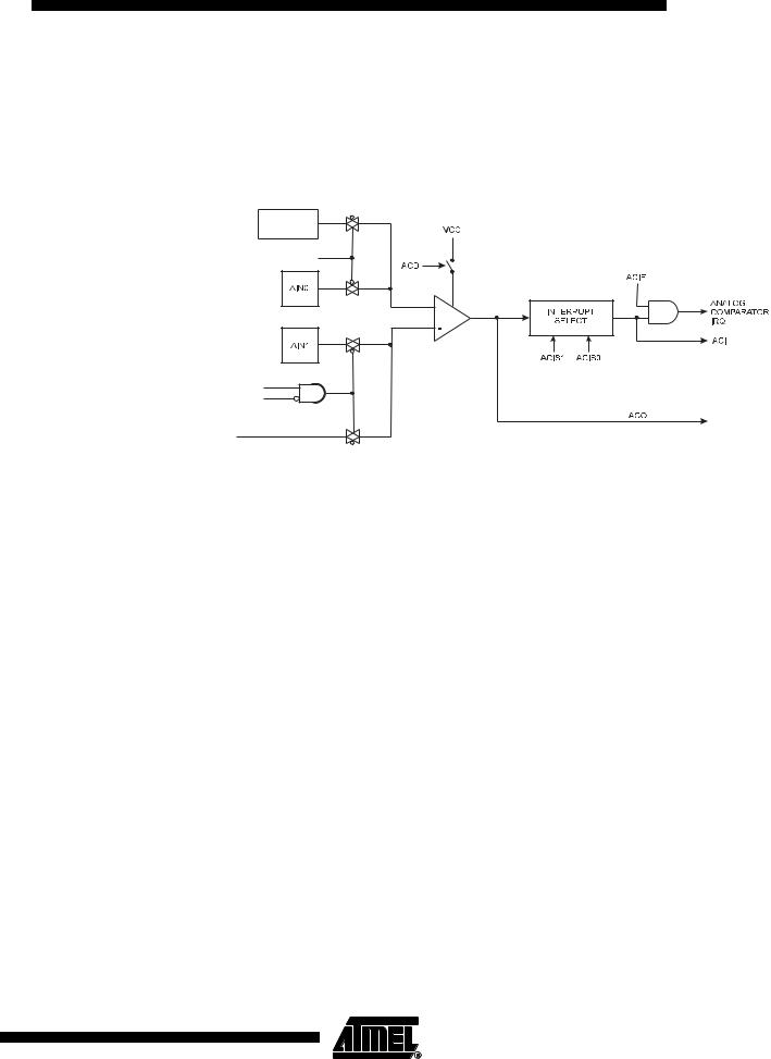
The Analog Comparator compares the input values on the positive pin AIN0 and negative pin AIN1. When the voltage on the positive pin AIN0 is higher than the voltage on the negative pin AIN1, the Analog Comparator output, ACO, is set. The comparator can trigger a separate interrupt, exclusive to the Analog Comparator. The user can select Interrupt triggering on comparator output rise, fall or toggle. A block diagram of the comparator and its surrounding logic is shown in Figure 38.
Figure 38. Analog Comparator Block Diagram(2)
BANDGAP
REFERENCE
ACBG
ACME
ADEN
ADC MULTIPLEXER
OUTPUT (1)
Notes: 1. See Table 36 on page 75.
2.Refer to Figure 1 on page 1 and Table 24 on page 49 for Analog Comparator pin placement.
Bit |
7 |
6 |
5 |
4 |
3 |
2 |
1 |
0 |
|
|
– |
ACME |
– |
– |
– |
ADTS2 |
ADTS1 |
ADTS0 |
ADCSRB |
Read/Write |
R |
R/W |
R |
R |
R |
R/W |
R/W |
R/W |
|
Initial Value |
0 |
0 |
0 |
0 |
0 |
0 |
0 |
0 |
|
• Bit 6 – ACME: Analog Comparator Multiplexer Enable
When this bit is written logic one and the ADC is switched off (ADEN in ADCSRA is zero), the ADC multiplexer selects the negative input to the Analog Comparator. When this bit is written logic zero, AIN1 is applied to the negative input of the Analog Comparator. For a detailed description of this bit, see “Analog Comparator Multiplexed Input” on page 75.
Bit |
7 |
6 |
5 |
4 |
3 |
2 |
1 |
0 |
|
|
ACD |
ACBG |
ACO |
ACI |
ACIE |
– |
ACIS1 |
ACIS0 |
ACSR |
|
|
|
|
|
|
|
|
|
|
Read/Write |
R/W |
R/W |
R |
R/W |
R/W |
R |
R/W |
R/W |
|
Initial Value |
0 |
0 |
N/A |
0 |
0 |
0 |
0 |
0 |
|
• Bit 7 – ACD: Analog Comparator Disable
When this bit is written logic one, the power to the Analog Comparator is switched off. This bit can be set at any time to turn off the Analog Comparator. This will reduce power consumption in Active and Idle mode. When changing the ACD bit, the Analog Comparator Interrupt must be disabled by clearing the ACIE bit in ACSR. Otherwise an interrupt can occur when the bit is changed.
73
2535A–AVR–06/03

• Bit 6 – ACBG: Analog Comparator Bandgap Select
When this bit is set, a fixed bandgap reference voltage replaces the positive input to the
Analog Comparator. When this bit is cleared, AIN0 is applied to the positive input of the
Analog Comparator.
• Bit 5 – ACO: Analog Comparator Output
The output of the Analog Comparator is synchronized and then directly connected to
ACO. The synchronization introduces a delay of 1 - 2 clock cycles.
• Bit 4 – ACI: Analog Comparator Interrupt Flag
This bit is set by hardware when a comparator output event triggers the interrupt mode defined by ACIS1 and ACIS0. The Analog Comparator interrupt routine is executed if the ACIE bit is set and the I-bit in SREG is set. ACI is cleared by hardware when executing the corresponding interrupt handling vector. Alternatively, ACI is cleared by writing a logic one to the flag.
• Bit 3 – ACIE: Analog Comparator Interrupt Enable
When the ACIE bit is written logic one and the I-bit in the Status Register is set, the Analog Comparator interrupt is activated. When written logic zero, the interrupt is disabled.
• Bit 2 – Res: Reserved Bit
This bit is a reserved bit in the ATtiny13 and will always read as zero.
• Bits 1, 0 – ACIS1, ACIS0: Analog Comparator Interrupt Mode Select
These bits determine which comparator events that trigger the Analog Comparator interrupt. The different settings are shown in Table 35.
Table 35. |
ACIS1/ACIS0 Settings |
||
ACIS1 |
|
ACIS0 |
Interrupt Mode |
|
|
|
|
0 |
|
0 |
Comparator Interrupt on Output Toggle. |
|
|
|
|
0 |
|
1 |
Reserved |
|
|
|
|
1 |
|
0 |
Comparator Interrupt on Falling Output Edge. |
|
|
|
|
1 |
|
1 |
Comparator Interrupt on Rising Output Edge. |
|
|
|
|
When changing the ACIS1/ACIS0 bits, the Analog Comparator Interrupt must be disabled by clearing its Interrupt Enable bit in the ACSR Register. Otherwise an interrupt can occur when the bits are changed.
74 ATtiny13
2535A–AVR–06/03