

8-bit Timer/Counter0 with PWM
Timer/Counter0 is a general purpose 8-bit Timer/Counter module, with two independent Output Compare Units, and with PWM support. It allows accurate program execution timing (event management) and wave generation. The main features are:
•Two Independent Output Compare Units
•Double Buffered Output Compare Registers
•Clear Timer on Compare Match (Auto Reload)
•Glitch Free, Phase Correct Pulse Width Modulator (PWM)
•Variable PWM Period
•Frequency Generator
•Three Independent Interrupt Sources (TOV0, OCF0A, and OCF0B)
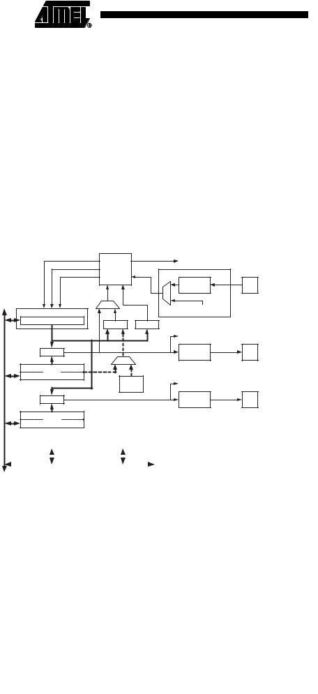
Overview |
A simplified block diagram of the 8-bit Timer/Counter is shown in Figure 25. For the |
|
actual placement of I/O pins, refer to “Pinout ATtiny13” on page 1. CPU accessible I/O |
|
Registers, including I/O bits and I/O pins, are shown in bold. The device-specific I/O |
|
Register and bit locations are listed in the “8-bit Timer/Counter Register Description” on |
|
page 65. |
Figure 25. 8-bit Timer/Counter Block Diagram
|
Count |
|
|
Clear |
|
|
Control Logic |
|
|
Direction |
clkTn |
|
TOP |
BOTTOM |
|
Timer/Counter |
|
|
TCNTn |
= 0 |
|
= |
|
|
= |
|
|
OCRnA |
|
|
|
Fixed |
|
|
TOP |
BUS |
|
Value |
= |
|
|
DATA |
OCRnB |
|
TOVn
(Int.Req.)
Clock Select
Edge
Tn
Detector
( From Prescaler )
OCnA
(Int.Req.)
Waveform
OCnA
Generation
OCnB
(Int.Req.)
Waveform
OCnB
Generation
|
TCCRnA |
|
TCCRnB |
|||
|
|
|
|
|
|
|
|
|
|
|
|
|
|
|
|
|
|
|
|
|
|
|
|
|
|
|
|
Registers |
The Timer/Counter (TCNT0) and Output Compare Registers (OCR0A and OCR0B) are |
|
|
|
8-bit registers. Interrupt request (abbreviated to Int.Req. in the figure) signals are all vis- |
|
|
ible in the Timer Interrupt Flag Register (TIFR0). All interrupts are individually masked |
|
|
with the Timer Interrupt Mask Register (TIMSK0). TIFR0 and TIMSK0 are not shown in |
|
|
the figure. |
|
|
The Timer/Counter can be clocked internally, via the prescaler, or by an external clock |
|
|
source on the T0 pin. The Clock Select logic block controls which clock source and edge |
|
|
the Timer/Counter uses to increment (or decrement) its value. The Timer/Counter is |
|
|
inactive when no clock source is selected. The output from the Clock Select logic is |
|
|
referred to as the timer clock (clkT0). |
|
|
The double buffered Output Compare Registers (OCR0A and OCR0B) is compared with |
|
|
the Timer/Counter value at all times. The result of the compare can be used by the |
|
|
Waveform Generator to generate a PWM or variable frequency output on the Output |
54 |
ATtiny13 |
|
|
||
|
||
2535A–AVR–06/03

|
|
|
|
ATtiny13 |
|
|
|
|
|
|
|
|
|
|
|
|
Compare pins (OC0A and OC0B). See “Output Compare Unit” on page 56. for details. |
||
|
|
The Compare Match event will also set the Compare Flag (OCF0A or OCF0B) which |
||
|
|
can be used to generate an Output Compare interrupt request. |
||
Definitions |
Many register and bit references in this section are written in general form. A lower case |
|||
|
|
“n” replaces the Timer/Counter number, in this case 0. A lower case “x” replaces the |
||
|
|
Output Compare Unit, in this case Compare Unit A or Compare Unit B. However, when |
||
|
|
using the register or bit defines in a program, the precise form must be used, i.e., |
||
|
|
TCNT0 for accessing Timer/Counter0 counter value and so on. |
||
|
|
The definitions in Table 26 are also used extensively throughout the document. |
||
|
|
Table 26. Definitions |
||
|
|
|
|
|
|
|
BOTTOM |
The counter reaches the BOTTOM when it becomes 0x00. |
|
|
|
MAX |
The counter reaches its MAXimum when it becomes 0xFF (decimal 255). |
|
|
|
TOP |
The counter reaches the TOP when it becomes equal to the highest |
|
|
|
|
value in the count sequence. The TOP value can be assigned to be the |
|
|
|
|
fixed value 0xFF (MAX) or the value stored in the OCR0A Register. The |
|
|
|
|
assignment is dependent on the mode of operation. |
|
|
|
|
|
|
Timer/Counter Clock
Sources
Counter Unit
The Timer/Counter can be clocked by an internal or an external clock source. The clock source is selected by the Clock Select logic which is controlled by the Clock Select (CS02:0) bits located in the Timer/Counter Control Register (TCCR0B). For details on clock sources and prescaler, see “Timer/Counter Prescaler” on page 71.
The main part of the 8-bit Timer/Counter is the programmable bi-directional counter unit. Figure 26 shows a block diagram of the counter and its surroundings.
Figure 26. Counter Unit Block Diagram
|
|
|
|
|
|
|
|
|
|
|
|
TOVn |
|
|
|
|
|
|
|
||||
|
|
DATA BUS |
|
|
|
|
|
|
|
|
(Int.Req.) |
|
|
|
|
|
|
|
|||||
|
|
|
|
|
|
|
|
|
|
|
|
|
|
|
|
|
|
|
|
|
|
|
|
|
|
|
|
|
|
|
|
|
|
|
|
|
|
|
|
|
Clock Select |
|
|
||||
|
|
|
|
|
|
count |
|
|
|
|
|
|
|
|
|
|
|
|
|
|
|
|
|
|
|
|
|
|
|
|
|
|
|
|
|
|
|
|
|
Edge |
|
|
|
Tn |
|||
|
|
|
TCNTn |
|
|
clear |
Control Logic |
clkTn |
|
|
|
Detector |
|
|
|
|
|||||||
|
|
|
|
|
|
|
|
|
|
|
|
||||||||||||
|
|
|
|
|
direction |
|
|
|
|
|
|
|
|
|
|
|
|
||||||
|
|
|
|
|
|
|
|
|
|
|
|
|
|
|
|
|
|
|
|
|
|
|
|
|
|
|
|
|
|
|
|
|
|
|
|
|
|
|
|
|
|
|
|
|
|
|
|
|
|
|
|
|
|
|
|
|
|
|
|
|
|
|
|
|
( From Prescaler ) |
|
|
|
|||
|
|
|
|
|
|
|
|
|
|
|
|
|
|
|
|
|
|
|
|||||
|
|
|
|
|
|
|
|
|
|
|
|
|
|
|
|
|
|
|
|
|
|
||
|
|
|
|
|
|
|
|
|
|
|
|
|
|
|
|
|
|
|
|
|
|
|
|
|
|
|
|
|
|
bottom |
|
top |
|
|
|
|
|
|
|
||||||||
Signal description (internal signals): |
|
|
|
|
|
|
|
|
|
|
|
|
|
|
|||||||||
count |
Increment or decrement TCNT0 by 1. |
|
|
|
|
|
|
|
|||||||||||||||
direction |
Select between increment and decrement. |
|
|
|
|
|
|
|
|||||||||||||||
clear |
Clear TCNT0 (set all bits to zero). |
|
|
|
|
|
|
|
|||||||||||||||
clkTn |
Timer/Counter clock, referred to as clkT0 in the following. |
|
|
||||||||||||||||||||
top |
Signalize that TCNT0 has reached maximum value. |
|
|
||||||||||||||||||||
bottom |
Signalize that TCNT0 has reached minimum value (zero). |
|
|
||||||||||||||||||||
55
2535A–AVR–06/03