

 ATtiny25/45/85
When using register indirect addressing modes with automatic pre-decrement and post-incre- ment, the address registers X, Y, and Z are decremented or incremented.
The 32 general purpose working registers, 64 I/O Registers, and the 128/256/512 bytes of internal data SRAM in the ATtiny25/45/85 are all accessible through all these addressing modes. The Register File is described in ”General Purpose Register File” on page 8.
Figure 5-2. Data Memory Map
Data Memory
32 Registers |
0x0000 - 0x001F |
64 I/O Registers |
0x0020 - 0x005F |
|
0x0060 |
Internal SRAM |
|
(128/256/512 x 8) |
|
|
0x0DF/0x015F/0x025F |
5.2.1Data Memory Access Times
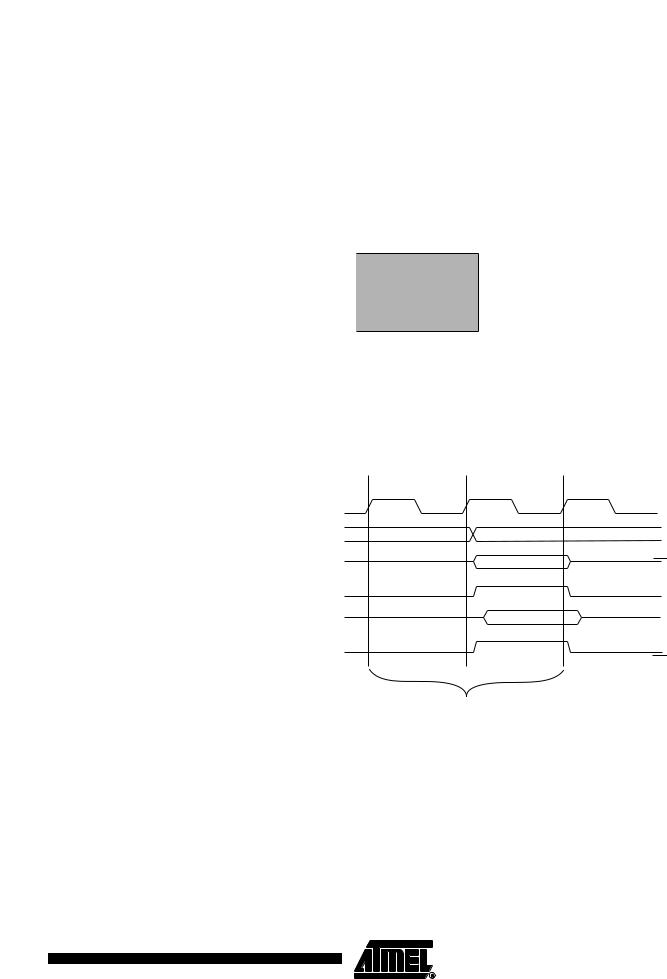
This section describes the general access timing concepts for internal memory access. The internal data SRAM access is performed in two clkCPU cycles as described in Figure 5-3.
Figure 5-3. On-chip Data SRAM Access Cycles
T1 T2 T3
clkCPU
Address Compute Address Address valid
Data
WR
Data
RD
 Read Write
Memory Access Instruction |
Next Instruction |
5.3EEPROM Data Memory
The ATtiny25/45/85 contains 128/256/512 bytes of data EEPROM memory. It is organized as a separate data space, in which single bytes can be read and written. The EEPROM has an endurance of at least 100,000 write/erase cycles. The access between the EEPROM and the CPU is described in the following, specifying the EEPROM Address Registers, the EEPROM Data Register, and the EEPROM Control Register. For a detailed description of Serial data downloading to the EEPROM, see page 153.
15
2586A–AVR–02/05

5.3.1EEPROM Read/Write Access
The EEPROM Access Registers are accessible in the I/O space.
The write access times for the EEPROM are given in Table 5-1. A self-timing function, however, lets the user software detect when the next byte can be written. If the user code contains instructions that write the EEPROM, some precautions must be taken. In heavily filtered power supplies, VCC is likely to rise or fall slowly on Power-up/down. This causes the device for some period of time to run at a voltage lower than specified as minimum for the clock frequency used. See ”Preventing EEPROM Corruption” on page 20 for details on how to avoid problems in these situations.
In order to prevent unintentional EEPROM writes, a specific write procedure must be followed. Refer to ”Atomic Byte Programming” on page 18 and ”Split Byte Programming” on page 18 for details on this.
When the EEPROM is read, the CPU is halted for four clock cycles before the next instruction is executed. When the EEPROM is written, the CPU is halted for two clock cycles before the next instruction is executed.
5.3.2EEPROM Address Register – EEARH and EEARL
Bit |
7 |
6 |
5 |
4 |
3 |
2 |
1 |
0 |
|
|
- |
- |
- |
- |
- |
- |
- |
EEAR8 |
EEARH |
|
|
|
|
|
|
|
|
|
|
|
EEAR7 |
EEAR6 |
EEAR5 |
EEAR4 |
EEAR3 |
EEAR2 |
EEAR1 |
EEAR0 |
EEARL |
|
|
|
|
|
|
|
|
|
|
Bit |
7 |
6 |
5 |
4 |
3 |
2 |
1 |
0 |
|
Read/Write |
R |
R |
R |
R |
R |
R |
R |
R/W |
|
Read/Write |
R/W |
R/W |
R/W |
R/W |
R/W |
R/W |
R/W |
R/W |
|
Initial Value |
0 |
0 |
0 |
0 |
0 |
0 |
0 |
X |
|
Initial Value |
X |
X |
X |
X |
X |
X |
X |
X |
|
• Bit 7..1 – Res6..0: Reserved Bits
These bits are reserved for future use and will always read as 0 in ATtiny25/45/85.
• Bits 8..0 – EEAR8..0: EEPROM Address
The EEPROM Address Registers – EEARH and EEARL – specifies the high EEPROM address in the 128/256/512 bytes EEPROM space. The EEPROM data bytes are addressed linearly between 0 and 127/255/511. The initial value of EEAR is undefined. A proper value must be written before the EEPROM may be accessed.
5.3.3EEPROM Data Register – EEDR
Bit |
7 |
6 |
5 |
4 |
3 |
2 |
1 |
0 |
|
|
EEDR7 |
EEDR6 |
EEDR5 |
EEDR4 |
EEDR3 |
EEDR2 |
EEDR1 |
EEDR0 |
EEDR |
|
|
|
|
|
|
|
|
|
|
Read/Write |
R/W |
R/W |
R/W |
R/W |
R/W |
R/W |
R/W |
R/W |
|
Initial Value |
0 |
0 |
0 |
0 |
0 |
0 |
0 |
0 |
|
• Bits 7..0 – EEDR7..0: EEPROM Data
For the EEPROM write operation the EEDR Register contains the data to be written to the EEPROM in the address given by the EEAR Register. For the EEPROM read operation, the EEDR contains the data read out from the EEPROM at the address given by EEAR.
16 ATtiny25/45/85
2586A–AVR–02/05

ATtiny25/45/85
5.3.4EEPROM Control Register – EECR
Bit |
7 |
6 |
5 |
4 |
3 |
2 |
1 |
0 |
|
|
– |
– |
EEPM1 |
EEPM0 |
EERIE |
EEMPE |
EEPE |
EERE |
EECR |
|
|
|
|
|
|
|
|
|
|
Read/Write |
R |
R |
R/W |
R/W |
R/W |
R/W |
R/W |
R/W |
|
Initial Value |
0 |
0 |
X |
X |
0 |
0 |
X |
0 |
|
• Bit 7 – Res: Reserved Bit
This bit is reserved for future use and will always read as 0 in ATtiny25/45/85. For compatibility with future AVR devices, always write this bit to zero. After reading, mask out this bit.
• Bit 6 – Res: Reserved Bit
This bit is reserved in the ATtiny25/45/85 and will always read as zero.
• Bits 5, 4 – EEPM1 and EEPM0: EEPROM Programming Mode Bits
The EEPROM Programming mode bits setting defines which programming action that will be triggered when writing EEPE. It is possible to program data in one atomic operation (erase the old value and program the new value) or to split the Erase and Write operations in two different operations. The Programming times for the different modes are shown in Table 5-1. While EEPE is set, any write to EEPMn will be ignored. During reset, the EEPMn bits will be reset to 0b00 unless the EEPROM is busy programming.
Table 5-1. |
EEPROM Mode Bits |
|
|
|
|
Programming |
|
EEPM1 |
EEPM0 |
Time |
Operation |
|
|
|
|
0 |
0 |
3.4 ms |
Erase and Write in one operation (Atomic Operation) |
|
|
|
|
0 |
1 |
1.8 ms |
Erase Only |
|
|
|
|
1 |
0 |
1.8 ms |
Write Only |
|
|
|
|
1 |
1 |
– |
Reserved for future use |
|
|
|
|
• Bit 3 – EERIE: EEPROM Ready Interrupt Enable
Writing EERIE to one enables the EEPROM Ready Interrupt if the I-bit in SREG is set. Writing EERIE to zero disables the interrupt. The EEPROM Ready Interrupt generates a constant interrupt when Non-volatile memory is ready for programming.
• Bit 2 – EEMPE: EEPROM Master Program Enable
The EEMPE bit determines whether writing EEPE to one will have effect or not.
When EEMPE is set, setting EEPE within four clock cycles will program the EEPROM at the selected address. If EEMPE is zero, setting EEPE will have no effect. When EEMPE has been written to one by software, hardware clears the bit to zero after four clock cycles.
• Bit 1 – EEPE: EEPROM Program Enable
The EEPROM Program Enable Signal EEPE is the programming enable signal to the EEPROM. When EEPE is written, the EEPROM will be programmed according to the EEPMn bits setting. The EEMPE bit must be written to one before a logical one is written to EEPE, otherwise no EEPROM write takes place. When the write access time has elapsed, the EEPE bit is cleared by hardware. When EEPE has been set, the CPU is halted for two cycles before the next instruction is executed.
17
2586A–AVR–02/05

• Bit 0 – EERE: EEPROM Read Enable
The EEPROM Read Enable Signal – EERE – is the read strobe to the EEPROM. When the correct address is set up in the EEAR Register, the EERE bit must be written to one to trigger the EEPROM read. The EEPROM read access takes one instruction, and the requested data is available immediately. When the EEPROM is read, the CPU is halted for four cycles before the next instruction is executed. The user should poll the EEPE bit before starting the read operation. If a write operation is in progress, it is neither possible to read the EEPROM, nor to change the EEAR Register.
5.3.5Atomic Byte Programming
Using Atomic Byte Programming is the simplest mode. When writing a byte to the EEPROM, the user must write the address into the EEARL Register and data into EEDR Register. If the EEPMn bits are zero, writing EEPE (within four cycles after EEMPE is written) will trigger the erase/write operation. Both the erase and write cycle are done in one operation and the total programming time is given in Table 1. The EEPE bit remains set until the erase and write operations are completed. While the device is busy with programming, it is not possible to do any other EEPROM operations.
5.3.6Split Byte Programming
It is possible to split the erase and write cycle in two different operations. This may be useful if the system requires short access time for some limited period of time (typically if the power supply voltage falls). In order to take advantage of this method, it is required that the locations to be written have been erased before the write operation. But since the erase and write operations are split, it is possible to do the erase operations when the system allows doing time-critical operations (typically after Power-up).
5.3.7Erase
To erase a byte, the address must be written to EEAR. If the EEPMn bits are 0b01, writing the EEPE (within four cycles after EEMPE is written) will trigger the erase operation only (programming time is given in Table 1). The EEPE bit remains set until the erase operation completes. While the device is busy programming, it is not possible to do any other EEPROM operations.
5.3.8Write
To write a location, the user must write the address into EEAR and the data into EEDR. If the EEPMn bits are 0b10, writing the EEPE (within four cycles after EEMPE is written) will trigger the write operation only (programming time is given in Table 1). The EEPE bit remains set until the write operation completes. If the location to be written has not been erased before write, the data that is stored must be considered as lost. While the device is busy with programming, it is not possible to do any other EEPROM operations.
The calibrated Oscillator is used to time the EEPROM accesses. Make sure the Oscillator frequency is within the requirements described in ”Oscillator Calibration Register – OSCCAL” on page 27.
The following code examples show one assembly and one C function for erase, write, or atomic write of the EEPROM. The examples assume that interrupts are controlled (e.g., by disabling interrupts globally) so that no interrupts will occur during execution of these functions.
18 ATtiny25/45/85 
2586A–AVR–02/05

ATtiny25/45/85
Assembly Code Example
EEPROM_write:
; Wait for completion of previous write sbic EECR,EEPE
rjmp EEPROM_write
; Set Programming mode
ldi r16, (0<<EEPM1)|(0<<EEPM0) out EECR, r16
; Set up address (r17) in address register out EEARL, r17
; Write data (r16) to data register out EEDR,r16
; Write logical one to EEMWE sbi EECR,EEMWE
; Start eeprom write by setting EEWE sbi EECR,EEWE
ret
C Code Example
void EEPROM_write(unsigned char ucAddress, unsigned char ucData)
{
/* Wait for completion of previous write */ while(EECR & (1<<EEPE))
;
/* Set Programming mode */
EECR = (0<<EEPM1)|(0>>EEPM0)
/* Set up address and data registers */ EEARL = ucAddress;
EEDR = ucData;
/* Write logical one to EEMWE */
EECR |= (1<<EEMWE);
/* Start eeprom write by setting EEWE */
EECR |= (1<<EEWE);
}
19
2586A–AVR–02/05