


22.7High-voltage Serial Programming
This section describes how to program and verify Flash Program memory, EEPROM Data memory, Lock bits and Fuse bits in the ATtiny25/45/85.
Figure 22-4. High-voltage Serial Programming
+11.5 - 12.5V |
|
|
|
|
+1.8 - 5.5V |
|||||
|
|
|
|
|
|
|
|
|
||
|
|
|
|
PB5 |
(RESET) |
|
VCC |
|
|
|
SCI |
|
|
PB3 |
PB2 |
|
|
SDO |
|||
|
|
|
||||||||
PB1  SII
SII
GND |
PB0 |
SDI |
Table 22-12. Pin Name Mapping
Signal Name in High-voltage |
|
|
|
Serial Programming Mode |
Pin Name |
I/O |
Function |
|
|
|
|
SDI |
PB0 |
I |
Serial Data Input |
|
|
|
|
SII |
PB1 |
I |
Serial Instruction Input |
|
|
|
|
SDO |
PB2 |
O |
Serial Data Output |
|
|
|
|
SCI |
PB3 |
I |
Serial Clock Input (min. 220ns period) |
|
|
|
|
The minimum period for the Serial Clock Input (SCI) during High-voltage Serial Programming is 220 ns.
Table 22-13. Pin Values Used to Enter Programming Mode
Pin |
Symbol |
Value |
|
|
|
SDI |
Prog_enable[0] |
0 |
|
|
|
SII |
Prog_enable[1] |
0 |
|
|
|
SDO |
Prog_enable[2] |
0 |
|
|
|
158 ATtiny25/45/85 
2586A–AVR–02/05

 ATtiny25/45/85
22.8High-voltage Serial Programming Algorithm
To program and verify the ATtiny25/45/85 in the High-voltage Serial Programming mode, the following sequence is recommended (See instruction formats in Table 22-15):
22.8.1Enter High-voltage Serial Programming Mode
The following algorithm puts the device in High-voltage Serial Programming mode:
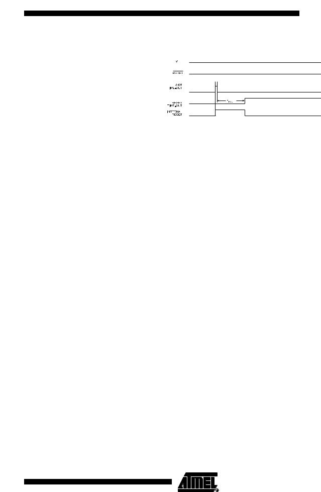
1.Set Prog_enable pins listed in Table 22-13 to “000”, RESET pin and VCC to 0V.
2.Apply 4.5 - 5.5V between VCC and GND.
Ensure that VCC reaches at least 1.8V within the next 20 µs.
3.Wait 20 - 60 µs, and apply 11.5 - 12.5V to RESET.
4.Keep the Prog_enable pins unchanged for at least 10 µs after the High-voltage has been applied to ensure the Prog_enable Signature has been latched.
5.Release the Prog_enable[2] pin to avoid drive contention on the Prog_enable[2]/SDO pin.
6.Wait at least 300 µs before giving any serial instructions on SDI/SII.
7.Exit Programming mode by power the device down or by bringing RESET pin to 0V.
If the rise time of the VCC is unable to fulfill the requirements listed above, the following alternative algorithm can be used:
1.Set Prog_enable pins listed in Table 22-13 to “000”, RESET pin and VCC to 0V.
2.Apply 4.5 - 5.5V between VCC and GND.
3.Monitor VCC, and as soon as VCC reaches 0.9 - 1.1V, apply 11.5 - 12.5V to RESET.
4.Keep the Prog_enable pins unchanged for at least 10 µs after the High-voltage has been applied to ensure the Prog_enable Signature has been latched.
5.Release the Prog_enable[2] pin to avoid drive contention on the Prog_enable[2]/SDO pin.
6.Wait until VCC actually reaches 4.5 - 5.5V before giving any serial instructions on SDI/SII.
7.Exit Programming mode by power the device down or by bringing RESET pin to 0V.
Table 22-14. High-voltage Reset Characteristics
|
|
Minimum High-voltage Period for |
Supply Voltage |
RESET Pin High-voltage Threshold |
Latching Prog_enable |
|
|
|
VCC |
VHVRST |
tHVRST |
4.5V |
11.5V |
100 ns |
|
|
|
5.5V |
11.5V |
100 ns |
|
|
|
22.8.2Considerations for Efficient Programming
The loaded command and address are retained in the device during programming. For efficient programming, the following should be considered.
•The command needs only be loaded once when writing or reading multiple memory locations.
•Skip writing the data value 0xFF that is the contents of the entire EEPROM (unless the EESAVE Fuse is programmed) and Flash after a Chip Erase.
159
2586A–AVR–02/05

•Address High byte needs only be loaded before programming or reading a new 256 word window in Flash or 256 byte EEPROM. This consideration also applies to Signature bytes reading.
22.8.3Chip Erase
The Chip Erase will erase the Flash and EEPROM(1) memories plus Lock bits. The Lock bits are not reset until the Program memory has been completely erased. The Fuse bits are not changed. A Chip Erase must be performed before the Flash and/or EEPROM are reprogrammed.
Note: 1. The EEPROM memory is preserved during Chip Erase if the EESAVE Fuse is programmed.
1.Load command “Chip Erase” (see Table 22-15).
2.Wait after Instr. 3 until SDO goes high for the “Chip Erase” cycle to finish.
3.Load Command “No Operation”.
22.8.4Programming the Flash
The Flash is organized in pages, see Table 22-10 on page 156. When programming the Flash, the program data is latched into a page buffer. This allows one page of program data to be programmed simultaneously. The following procedure describes how to program the entire Flash memory:
1.Load Command “Write Flash” (see Table 22-15).
2.Load Flash Page Buffer.
3.Load Flash High Address and Program Page. Wait after Instr. 3 until SDO goes high for the “Page Programming” cycle to finish.
4.Repeat 2 through 3 until the entire Flash is programmed or until all data has been programmed.
5.End Page Programming by Loading Command “No Operation”.
When writing or reading serial data to the ATtiny25/45/85, data is clocked on the rising edge of the serial clock, see Figure 22-6, Figure 22-7 and Table 22-16 for details.
Figure 22-5. Addressing the Flash which is Organized in Pages
|
PROGRAM |
PCMSB |
|
|
|
|
PAGEMSB |
|
|||||||
|
|
PCPAGE |
PCWORD |
|
|
|
|
||||||||
|
COUNTER |
|
|
|
|
|
|||||||||
|
|
|
|
|
|
|
|
|
|
|
|
|
|
||
|
PAGE ADDRESS |
|
|
WORD ADDRESS |
|
||||||||||
|
WITHIN THE FLASH |
|
|
WITHIN A PAGE |
|
||||||||||
PROGRAM MEMORY |
|
|
|
|
|
|
|
|
|
PAGE |
PCWORD[PAGEMSB:0]: |
||||
|
|
|
|
|
|
|
|
|
|
|
|
|
|
|
|
|
PAGE |
|
|
|
|
|
|
|
|
INSTRUCTION WORD |
00 |
||||
|
|
|
|
|
|
|
|
|
|
|
|
||||
|
|
|
|
|
|
|
|
|
|
|
|
|
|
|
01 |
|
|
|
|
|
|
|
|
|
|
|
|
|
|
|
|
|
|
|
|
|
|
|
|
|
|
|
|
|
|
|
02 |
|
|
|
|
|
|
|
|
|
|
|
|
|
|
|
|
|
|
|
|
|
|
|
|
|
|
|
|
|
|
|
|
|
|
|
|
|
|
|
|
|
|
|
|
|
|
|
|
|
|
|
|
|
|
|
|
|
|
|
|
|
|
|
|
|
|
|
|
|
|
|
|
|
|
|
|
|
|
|
|
|
|
|
|
|
|
|
|
|
|
|
|
|
|
|
|
|
|
|
|
|
|
|
|
|
|
|
|
|
|
|
|
|
|
|
|
|
|
|
|
|
|
|
|
|
|
|
|
|
|
|
|
|
|
|
|
|
|
|
|
|
|
|
|
|
|
|
|
|
|
|
|
|
|
|
|
|
|
|
|
|
|
|
|
|
|
|
|
|
|
|
|
|
|
|
|
|
|
|
|
|
|
|
|
|
|
|
|
|
|
|
|
|
|
|
|
|
|
|
|
|
|
|
|
|
|
|
|
|
|
|
|
|
|
|
|
|
|
|
|
|
|
|
|
PAGEEND
160 ATtiny25/45/85
2586A–AVR–02/05
ATtiny25/45/85
Figure 22-6. High-voltage Serial Programming Waveforms
SDI |
|
MSB |
|
|
|
|
|
|
LSB |
|
|
PB0 |
|
|
|
|
|
|
|
|
|
|
|
SII |
|
MSB |
|
|
|
|
|
|
LSB |
|
|
PB1 |
|
|
|
|
|
|
|
|
|
||
|
|
|
|
|
|
|
|
|
|
|
|
SDO |
|
MSB |
|
|
|
|
|
|
LSB |
|
|
PB2 |
|
|
|
|
|
|
|
|
|
|
|
SCI |
0 |
1 |
2 |
3 |
4 |
5 |
6 |
7 |
8 |
9 |
10 |
PB3 |
|
|
|
|
|
|
|
|
|
|
|
22.8.5Programming the EEPROM
The EEPROM is organized in pages, see Table 22-11 on page 157. When programming the EEPROM, the data is latched into a page buffer. This allows one page of data to be programmed simultaneously. The programming algorithm for the EEPROM Data memory is as follows (refer to Table 22-15):
1.Load Command “Write EEPROM”.
2.Load EEPROM Page Buffer.
3.Program EEPROM Page. Wait after Instr. 2 until SDO goes high for the “Page Programming” cycle to finish.
4.Repeat 2 through 3 until the entire EEPROM is programmed or until all data has been programmed.
5.End Page Programming by Loading Command “No Operation”.
22.8.6Reading the Flash
The algorithm for reading the Flash memory is as follows (refer to Table 22-15):
1.Load Command "Read Flash".
2.Read Flash Low and High Bytes. The contents at the selected address are available at serial output SDO.
22.8.7Reading the EEPROM
The algorithm for reading the EEPROM memory is as follows (refer to Table 22-15):
1.Load Command “Read EEPROM”.
2.Read EEPROM Byte. The contents at the selected address are available at serial output SDO.
22.8.8Programming and Reading the Fuse and Lock Bits
The algorithms for programming and reading the Fuse Low/High bits and Lock bits are shown in
Table 22-15.
22.8.9Reading the Signature Bytes and Calibration Byte
The algorithms for reading the Signature bytes and Calibration byte are shown in Table 22-15.
22.8.10Power-off sequence
Set SCI to “0”. Set RESET to “1”. Turn VCC power off.
161
2586A–AVR–02/05

Table 22-15. High-voltage Serial Programming Instruction Set for ATtiny25/45/85
|
|
|
Instruction Format |
|
|
||
|
|
|
|
|
|
|
|
Instruction |
|
Instr.1/5 |
Instr.2/6 |
Instr.3 |
Instr.4 |
Operation Remarks |
|
|
|
|
|
|
|
|
|
|
SD |
|
|
|
|
|
|
|
I |
0_1000_0000_00 |
0_0000_0000_00 |
0_0000_0000_00 |
|
Wait after Instr.3 until SDO goes |
|
Chip Erase |
SII |
0_0100_1100_00 |
0_0110_0100_00 |
0_0110_1100_00 |
|
high for the Chip Erase cycle to |
|
|
SD |
x_xxxx_xxxx_xx |
x_xxxx_xxxx_xx |
x_xxxx_xxxx_xx |
|
finish. |
|
|
O |
|
|
|
|
|
|
|
|
|
|
|
|
|
|
|
SD |
|
|
|
|
|
|
Load “Write |
I |
0_0001_0000_00 |
|
|
|
|
|
Flash” |
SII |
0_0100_1100_00 |
|
|
|
Enter Flash Programming code. |
|
Command |
SD |
x_xxxx_xxxx_xx |
|
|
|
|
|
|
O |
|
|
|
|
|
|
|
|
|
|
|
|
|
|
|
SD |
0_ bbbb_bbbb |
|
|
|
Repeat after Instr. 1 - 5 until the |
|
|
I |
0_eeee_eeee_00 |
0_dddd_dddd_00 |
0_0000_0000_00 |
|||
|
_00 |
entire page buffer is filled or until |
|||||
|
SII |
0_0010_1100_00 |
0_0011_1100_00 |
0_0111_1101_00 |
|||
|
0_0000_1100_00 |
all data within the page is filled. |
|||||
|
SD |
x_xxxx_xxxx_xx |
x_xxxx_xxxx_xx |
x_xxxx_xxxx_xx |
|||
|
x_xxxx_xxxx_xx |
See Note 1. |
|||||
Load Flash |
O |
|
|
|
|||
|
|
|
|
|
|||
|
|
|
|
|
|
||
Page Buffer |
SD |
|
|
|
|
|
|
|
|
|
|
|
|
||
|
I |
0_0000_0000_00 |
|
|
|
|
|
|
SII |
0_0111_1100_00 |
|
|
|
Instr 5. |
|
|
SD |
x_xxxx_xxxx_xx |
|
|
|
|
|
|
O |
|
|
|
|
|
|
|
|
|
|
|
|
|
|
|
SD |
|
|
|
|
Wait after Instr 3 until SDO goes |
|
Load Flash |
|
|
|
|
high. Repeat Instr. 2 - 3 for each |
||
I |
0_0000_000a_00 |
0_0000_0000_00 |
0_0000_0000_00 |
|
|||
High Address |
|
loaded Flash Page until the entire |
|||||
SII |
0_0001_1100_00 |
0_0110_0100_00 |
0_0110_1100_00 |
|
|||
and Program |
|
Flash or all data is programmed. |
|||||
SD |
x_xxxx_xxxx_xx |
x_xxxx_xxxx_xx |
x_xxxx_xxxx_xx |
|
|||
Page |
|
Repeat Instr. 1 for a new 256 byte |
|||||
O |
|
|
|
|
|||
|
|
|
|
|
page. See Note 1. |
||
|
|
|
|
|
|
||
|
|
|
|
|
|
|
|
|
SD |
|
|
|
|
|
|
Load “Read |
I |
0_0000_0010_00 |
|
|
|
|
|
Flash” |
SII |
0_0100_1100_00 |
|
|
|
Enter Flash Read mode. |
|
Command |
SD |
x_xxxx_xxxx_xx |
|
|
|
|
|
|
O |
|
|
|
|
|
|
|
|
|
|
|
|
|
|
|
SD |
0_bbbb_bbbb_0 |
|
|
|
|
|
|
I |
0_0000_000a_00 |
0_0000_0000_00 |
0_0000_0000_00 |
Repeat Instr. 1, 3 - 6 for each new |
||
|
0 |
||||||
|
SII |
0_0001_1100_00 |
0_0110_1000_00 |
0_0110_1100_00 |
address. Repeat Instr. 2 for a new |
||
|
0_0000_1100_00 |
||||||
|
SD |
x_xxxx_xxxx_xx |
x_xxxx_xxxx_xx |
q_qqqq_qqqx_xx |
256 byte page. |
||
Read Flash |
x_xxxx_xxxx_xx |
||||||
O |
|
|
|
|
|||
|
|
|
|
|
|||
Low and High |
|
|
|
|
|
|
|
SD |
|
|
|
|
|
||
Bytes |
|
|
|
|
|
||
|
I |
0_0000_0000_00 |
0_0000_0000_00 |
|
|
|
|
|
SII |
0_0111_1000_00 |
0_0111_1100_00 |
|
|
Instr 5 - 6. |
|
|
SD |
x_xxxx_xxxx_xx |
p_pppp_pppx_xx |
|
|
|
|
|
O |
|
|
|
|
|
|
|
|
|
|
|
|
|
|
|
SD |
|
|
|
|
|
|
Load “Write |
I |
0_0001_0001_00 |
|
|
|
Enter EEPROM Programming |
|
EEPROM” |
SII |
0_0100_1100_00 |
|
|
|
||
|
|
|
mode. |
||||
Command |
SD |
x_xxxx_xxxx_xx |
|
|
|
||
|
|
|
|
||||
|
O |
|
|
|
|
|
|
|
|
|
|
|
|
|
|
162 ATtiny25/45/85 
2586A–AVR–02/05

|
|
|
|
|
|
|
|
|
|
|
ATtiny25/45/85 |
|
|
|
|
|
|
|
|
|
|
|
|
|
|
|
|
|
|
|
|
|
|
|
|
|
Table 22-15. High-voltage Serial Programming Instruction Set for ATtiny25/45/85 (Continued) |
||||||||||
|
|||||||||||
|
|
|
|
|
|
|
|
||||
|
|
|
|
Instruction Format |
|
|
|||||
|
|
|
|
|
|
|
|
|
|
||
|
Instruction |
|
Instr.1/5 |
Instr.2/6 |
|
|
Instr.3 |
Instr.4 |
Operation Remarks |
||
|
|
|
|
|
|
|
|
|
|
|
|
|
|
SD |
0_00bb_bbbb_0 |
|
|
|
|
|
|
|
Repeat Instr. 1 - 4 until the entire |
|
Load |
I |
0_eeee_eeee_00 |
0_0000_0000_00 |
0_0000_0000_00 |
||||||
|
0 |
page buffer is filled or until all |
|||||||||
|
EEPROM |
SII |
0_0010_1100_00 |
0_0110_1101_00 |
0_0110_1100_00 |
||||||
|
0_0000_1100_00 |
data within the page is filled. See |
|||||||||
|
Page Buffer |
SD |
x_xxxx_xxxx_xx |
x_xxxx_xxxx_xx |
x_xxxx_xxxx_xx |
||||||
|
x_xxxx_xxxx_xx |
Note 2. |
|||||||||
|
|
O |
|
|
|
|
|
|
|
||
|
|
|
|
|
|
|
|
|
|
|
|
|
|
|
|
|
|
|
|
|
|
|
|
|
|
SD |
|
|
|
|
|
|
|
|
Wait after Instr. 2 until SDO goes |
|
Program |
I |
0_0000_0000_00 |
0_0000_0000_00 |
|
|
|
|
|
high. Repeat Instr. 1 - 2 for each |
|
|
EEPROM |
SII |
0_0110_0100_00 |
0_0110_1100_00 |
|
|
|
|
|
loaded EEPROM page until the |
|
|
Page |
SD |
x_xxxx_xxxx_xx |
x_xxxx_xxxx_xx |
|
|
|
|
|
entire EEPROM or all data is |
|
|
|
O |
|
|
|
|
|
|
|
|
programmed. |
|
|
|
|
|
|
|
|
|
|
|
|
|
|
SD |
0_00bb_bbbb_0 |
|
|
|
|
|
|
|
|
|
|
I |
0_eeee_eeee_00 |
0_0000_0000_00 |
0_0000_0000_00 |
Repeat Instr. 1 - 5 for each new |
|||||
|
|
0 |
|||||||||
|
|
SII |
0_0010_1100_00 |
0_0110_1101_00 |
0_0110_0100_00 |
address. Wait after Instr. 5 until |
|||||
|
|
0_0000_1100_00 |
|||||||||
|
|
SD |
x_xxxx_xxxx_xx |
x_xxxx_xxxx_xx |
x_xxxx_xxxx_xx |
SDO goes high. See Note 3. |
|||||
|
Write |
x_xxxx_xxxx_xx |
|||||||||
|
O |
|
|
|
|
|
|
|
|
||
|
|
|
|
|
|
|
|
|
|
||
|
EEPROM |
|
|
|
|
|
|
|
|
|
|
|
SD |
|
|
|
|
|
|
|
|
|
|
|
Byte |
|
|
|
|
|
|
|
|
|
|
|
|
I |
0_0000_0000_00 |
|
|
|
|
|
|
|
|
|
|
SII |
0_0110_1100_00 |
|
|
|
|
|
|
|
Instr. 5 |
|
|
SD |
x_xxxx_xxxx_xx |
|
|
|
|
|
|
|
|
|
|
O |
|
|
|
|
|
|
|
|
|
|
|
|
|
|
|
|
|
|
|
|
|
|
|
SD |
|
|
|
|
|
|
|
|
|
|
Load “Read |
I |
0_0000_0011_00 |
|
|
|
|
|
|
|
|
|
EEPROM” |
SII |
0_0100_1100_00 |
|
|
|
|
|
|
|
Enter EEPROM Read mode. |
|
Command |
SD |
x_xxxx_xxxx_xx |
|
|
|
|
|
|
|
|
|
|
O |
|
|
|
|
|
|
|
|
|
|
|
|
|
|
|
|
|
|
|
|
|
|
|
SD |
0_bbbb_bbbb_0 |
|
|
|
|
|
|
|
|
|
Read |
I |
0_aaaa_aaaa_00 |
0_0000_0000_00 |
0_0000_0000_00 |
Repeat Instr. 1, 3 - 4 for each new |
|||||
|
0 |
||||||||||
|
EEPROM |
SII |
0_0001_1100_00 |
0_0110_1000_00 |
0_0110_1100_00 |
address. Repeat Instr. 2 for a new |
|||||
|
0_0000_1100_00 |
||||||||||
|
Byte |
SD |
x_xxxx_xxxx_xx |
x_xxxx_xxxx_xx |
q_qqqq_qqq0_00 |
256 byte page. |
|||||
|
x_xxxx_xxxx_xx |
||||||||||
|
|
O |
|
|
|
|
|
|
|
|
|
|
|
|
|
|
|
|
|
|
|
|
|
|
|
|
|
|
|
|
|
|
|
|
|
|
|
SD |
|
|
|
|
|
|
|
|
|
|
Write Fuse |
I |
0_0100_0100_00 |
0_A987_6543_00 |
0_0000_0000_00 |
0_0000_0000_00 |
Wait after Instr. 4 until SDO goes |
||||
|
SII |
0_0100_1100_00 |
0_0010_1100_00 |
0_0110_0100_00 |
0_0110_1100_00 |
high. Write A - 3 = “0” to program |
|||||
|
Low Bits |
||||||||||
|
SD |
x_xxxx_xxxx_xx |
x_xxxx_xxxx_xx |
x_xxxx_xxxx_xx |
x_xxxx_xxxx_xx |
the Fuse bit. |
|||||
|
|
||||||||||
|
|
O |
|
|
|
|
|
|
|
|
|
|
|
|
|
|
|
|
|
|
|
|
|
|
|
SD |
|
0_000F_EDCB_0 |
|
|
|
|
|
|
|
|
|
I |
0_0100_0000_00 |
0_0000_0000_00 |
0_0000_0000_00 |
Wait after Instr. 4 until SDO goes |
|||||
|
Write Fuse |
0 |
|
||||||||
|
SII |
0_0100_1100_00 |
|
0_0111_0100_00 |
0_0111_1100_00 |
high. Write F - B = “0” to program |
|||||
|
High Bits |
0_0010_1100_00 |
|||||||||
|
SD |
x_xxxx_xxxx_xx |
x_xxxx_xxxx_xx |
x_xxxx_xxxx_xx |
the Fuse bit. |
||||||
|
|
x_xxxx_xxxx_xx |
|||||||||
|
|
O |
|
|
|
|
|
|
|
||
|
|
|
|
|
|
|
|
|
|
|
|
|
|
|
|
|
|
|
|
|
|
|
|
|
|
SD |
|
|
|
|
|
|
|
|
|
|
Write Lock |
I |
0_0010_0000_00 |
0_0000_0021_00 |
0_0000_0000_00 |
0_0000_0000_00 |
Wait after Instr. 4 until SDO goes |
||||
|
SII |
0_0100_1100_00 |
0_0010_1100_00 |
0_0110_0100_00 |
0_0110_1100_00 |
high. Write 2 - 1 = “0” to program |
|||||
|
Bits |
||||||||||
|
SD |
x_xxxx_xxxx_xx |
x_xxxx_xxxx_xx |
x_xxxx_xxxx_xx |
x_xxxx_xxxx_xx |
the Lock Bit. |
|||||
|
|
||||||||||
|
|
O |
|
|
|
|
|
|
|
|
|
|
|
|
|
|
|
|
|
|
|
|
|
|
|
SD |
|
|
|
|
|
|
|
|
|
|
Read Fuse |
I |
0_0000_0100_00 |
0_0000_0000_00 |
0_0000_0000_00 |
|
Reading A - 3 = “0” means the |
||||
|
SII |
0_0100_1100_00 |
0_0110_1000_00 |
0_0110_1100_00 |
|
||||||
|
Low Bits |
|
Fuse bit is programmed. |
||||||||
|
SD |
x_xxxx_xxxx_xx |
x_xxxx_xxxx_xx |
A_9876_543x_xx |
|
||||||
|
|
|
|
||||||||
|
|
O |
|
|
|
|
|
|
|
|
|
|
|
|
|
|
|
|
|
|
|
|
|
|
|
|
|
|
|
|
|
|
|
|
163 |
|
|
|
|
|
|
|
|
|
|
|
|
|
|
|
|
|
|
|
|
|
|
|
|
2586A–AVR–02/05

Table 22-15. High-voltage Serial Programming Instruction Set for ATtiny25/45/85 (Continued)
|
|
|
Instruction Format |
|
|
||
|
|
|
|
|
|
|
|
Instruction |
|
Instr.1/5 |
Instr.2/6 |
Instr.3 |
Instr.4 |
Operation Remarks |
|
|
|
|
|
|
|
|
|
|
SD |
|
|
|
|
|
|
Read Fuse |
I |
0_0000_0100_00 |
0_0000_0000_00 |
0_0000_0000_00 |
|
Reading F - B = “0” means the |
|
SII |
0_0100_1100_00 |
0_0111_1010_00 |
0_0111_1110_00 |
|
|||
High Bits |
|
Fuse bit is programmed. |
|||||
SD |
x_xxxx_xxxx_xx |
x_xxxx_xxxx_xx |
x_xxFE_DCBx_xx |
|
|||
|
|
|
|||||
|
O |
|
|
|
|
|
|
|
|
|
|
|
|
|
|
|
SD |
|
|
|
|
|
|
Read Lock |
I |
0_0000_0100_00 |
0_0000_0000_00 |
0_0000_0000_00 |
|
Reading 2, 1 = “0” means the |
|
SII |
0_0100_1100_00 |
0_0111_1000_00 |
0_0111_1100_00 |
|
|||
Bits |
|
Lock bit is programmed. |
|||||
SD |
x_xxxx_xxxx_xx |
x_xxxx_xxxx_xx |
x_xxxx_x21x_xx |
|
|||
|
|
|
|||||
|
O |
|
|
|
|
|
|
|
|
|
|
|
|
|
|
|
SD |
|
|
|
|
|
|
Read |
I |
0_0000_1000_00 |
0_0000_00bb_00 |
0_0000_0000_00 |
0_0000_0000_00 |
Repeats Instr 2 4 for each |
|
Signature |
SII |
0_0100_1100_00 |
0_0000_1100_00 |
0_0110_1000_00 |
0_0110_1100_00 |
||
signature byte address. |
|||||||
Bytes |
SD |
x_xxxx_xxxx_xx |
x_xxxx_xxxx_xx |
x_xxxx_xxxx_xx |
q_qqqq_qqqx_xx |
||
|
|||||||
|
O |
|
|
|
|
|
|
|
|
|
|
|
|
|
|
|
SD |
|
|
|
|
|
|
Read |
I |
0_0000_1000_00 |
0_0000_0000_00 |
0_0000_0000_00 |
0_0000_0000_00 |
|
|
Calibration |
SII |
0_0100_1100_00 |
0_0000_1100_00 |
0_0111_1000_00 |
0_0111_1100_00 |
|
|
Byte |
SD |
x_xxxx_xxxx_xx |
x_xxxx_xxxx_xx |
x_xxxx_xxxx_xx |
p_pppp_pppx_xx |
|
|
|
O |
|
|
|
|
|
|
|
|
|
|
|
|
|
|
|
SD |
|
|
|
|
|
|
Load “No |
I |
0_0000_0000_00 |
|
|
|
|
|
Operation” |
SII |
0_0100_1100_00 |
|
|
|
|
|
Command |
SD |
x_xxxx_xxxx_xx |
|
|
|
|
|
|
O |
|
|
|
|
|
|
|
|
|
|
|
|
|
|
Note: a = address high bits, b = address low bits, d = data in high bits, e = data in low bits, p = data out high bits, q = data out low bits, x = don’t care, 1 = Lock Bit1, 2 = Lock Bit2, 3 = CKSEL0 Fuse, 4 = CKSEL1 Fuse, 5 = SUT0 Fuse, 6 = SUT1 Fuse, 7 = CKDIV8, Fuse, 8 = WDTON Fuse, 9 = EESAVE Fuse, A = SPIEN Fuse, B = RSTDISBL Fuse, C = BODLEVEL0 Fuse, D= BODLEVEL1 Fuse, E = MONEN Fuse, F = SPMEN Fuse
Notes: 1. For page sizes less than 256 words, parts of the address (bbbb_bbbb) will be parts of the page address.
2.For page sizes less than 256 bytes, parts of the address (bbbb_bbbb) will be parts of the page address.
3.The EEPROM is written page-wise. But only the bytes that are loaded into the page are actually written to the EEPROM. Page-wise EEPROM access is more efficient when multiple bytes are to be written to the same page. Note that auto-erase of EEPROM is not available in High-voltage Serial Programming, only in SPI Programming.
164 ATtiny25/45/85 
2586A–AVR–02/05
ATtiny25/45/85
22.9High-voltage Serial Programming Characteristics
Figure 22-7. High-voltage Serial Programming Timing
CC


 CK
CK 

Table 22-16. High-voltage Serial Programming Characteristics TA = 25°C ± 10%, VCC = 5.0V ± 10% (Unless otherwise noted)
Symbol |
Parameter |
Min |
Typ |
Max |
Units |
|
|
|
|
|
|
tSHSL |
SCI (PB3) Pulse Width High |
110 |
|
|
ns |
tSLSH |
SCI (PB3) Pulse Width Low |
110 |
|
|
ns |
tIVSH |
SDI (PB0), SII (PB1) Valid to SCI (PB3) High |
50 |
|
|
ns |
tSHIX |
SDI (PB0), SII (PB1) Hold after SCI (PB3) High |
50 |
|
|
ns |
tSHOV |
SCI (PB3) High to SDO (PB2) Valid |
|
16 |
|
ns |
tWLWH_PFB |
Wait after Instr. 3 for Write Fuse Bits |
|
2.5 |
|
ms |
165
2586A–AVR–02/05