

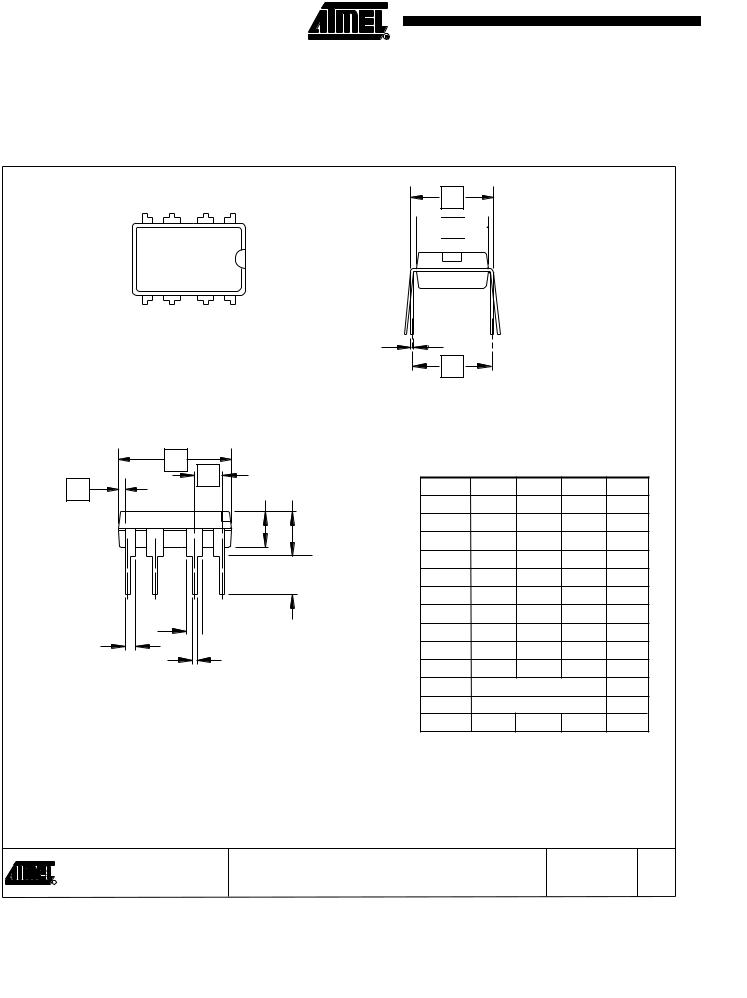
28. Packaging Information
28.18P3
1 |
E |
|

 E1
E1 

|
N |
Top View |
c |
|
eA |
|
End View |
D
e
D1 |
A2 A |
 b2 L
b2 L
b3
4 PLCS |
b |
Side View
COMMON DIMENSIONS
(Unit of Measure = inches)
SYMBOL |
MIN |
NOM |
MAX |
NOTE |
A |
|
|
0.210 |
2 |
A2 |
0.115 |
0.130 |
0.195 |
|
b |
0.014 |
0.018 |
0.022 |
5 |
b2 |
0.045 |
0.060 |
0.070 |
6 |
b3 |
0.030 |
0.039 |
0.045 |
6 |
c |
0.008 |
0.010 |
0.014 |
|
D |
0.355 |
0.365 |
0.400 |
3 |
D1 |
0.005 |
|
|
3 |
E |
0.300 |
0.310 |
0.325 |
4 |
E1 |
0.240 |
0.250 |
0.280 |
3 |
e |
|
0.100 BSC |
|
|
eA |
|
0.300 BSC |
|
4 |
L |
0.115 |
0.130 |
0.150 |
2 |
Notes: 1. This drawing is for general information only; refer to JEDEC Drawing MS-001, Variation BA for additional information.
2.Dimensions A and L are measured with the package seated in JEDEC seating plane Gauge GS-3.
3.D, D1 and E1 dimensions do not include mold Flash or protrusions. Mold Flash or protrusions shall not exceed 0.010 inch.
4.E and eA measured with the leads constrained to be perpendicular to datum.
5.Pointed or rounded lead tips are preferred to ease insertion.
6.b2 and b3 maximum dimensions do not include Dambar protrusions. Dambar protrusions shall not exceed 0.010 (0.25 mm).
|
|
01/09/02 |
||
2325 Orchard Parkway |
TITLE |
DRAWING NO. |
REV. |
|
8P3, 8-lead, 0.300" Wide Body, Plastic Dual |
8P3 |
B |
||
R San Jose, CA 95131 |
In-line Package (PDIP) |
|||
|
|
|||
178 ATtiny25/45/85 
2586A–AVR–02/05

ATtiny25/45/85
28.28S2
C 
1
E |
E1 |
N |
L |
|
|
|
|
Top View |
|
|
|
|
|
|
|
|
|
|
|
|
|||||||
|
|
|
|
|
|
|
|
|
|
|
|
|
||||||||||
|
|
|
|
|
|
|
|
|
|
|
|
|
|
|
End View |
|
|
|
|
|||
e |
|
|
|
|
|
|
|
|
|
b |
|
|
|
|
COMMON DIMENSIONS |
|
||||||
|
|
|
|
|
|
|
|
|
|
|
|
|
|
|||||||||
|
|
|
|
|
|
|
|
|
|
|
|
|
|
|
|
|
|
|
|
|||
|
|
|
|
|
|
|
|
|
|
|
A |
|
|
|
|
(Unit of Measure = mm) |
|
|||||
|
|
|
|
|
|
|
|
|
|
|
|
|
A1 |
|
|
|
SYMBOL |
MIN |
NOM |
MAX |
NOTE |
|
|
|
|
|
|
|
|
|
|
|
|
|
|
|
|
|
|||||||
|
|
|
|
|
|
|
|
|
|
|
|
|
|
|
|
A |
1.70 |
|
2.16 |
|
||
|
|
|
|
|
|
|
|
|
|
|
|
|
|
|
|
|
|
|||||
|
|
|
|
|
|
|
|
|
|
|
|
|
|
|
|
|
|
|
|
|
|
|
|
|
|
|
|
|
|
|
|
|
|
|
|
|
|
|
|
|
A1 |
0.05 |
|
0.25 |
|
|
|
|
|
|
|
|
|
|
|
|
|
|
|
|
|
|
|
b |
0.35 |
|
0.48 |
5 |
|
|
|
|
|
|
|
|
|
|
|
|
|
|
|
|
|
|
|
||||
|
|
|
|
|
|
|
|
|
|
|
|
|
|
|
|
|
|
|
|
|
|
|
|
|
|
|
|
|
|
|
|
|
|
|
|
|
|
|
|
|
C |
0.15 |
|
0.35 |
5 |
|
|
|
|
|
|
|
|
|
|
|
|
|
|
|
|
|
|
|
|
|
|
|
|
|
|
|
|
|
D |
|
|
|
|
|
|
|
|
|
|
D |
5.13 |
|
5.35 |
|
|
|
|
|
|
|
|
|
|
|
|
|
|
|
|
|
|
|
|
|||||
|
|
|
|
|
|
|
|
|
|
|
|
|
|
|
|
E1 |
5.18 |
|
5.40 |
2, 3 |
||
|
|
|
|
|
|
|
|
|
|
|
|
|
|
|
|
|
|
|
||||
|
|
|
|
|
|
|
|
|
|
|
|
|
|
|
|
|
|
|
|
|
|
|
|
|
|
|
|
Side View |
|
|
|
|
|
|
|
|
E |
7.70 |
|
8.26 |
|
||||
|
|
|
|
|
|
|
|
|
|
|
|
|
|
|
|
|
|
|||||
|
|
|
|
|
|
|
|
L |
0.51 |
|
0.85 |
|
||||||||||
|
|
|
|
|
|
|
|
|
|
|
|
|
|
|
|
|
|
|
|
|||
|
|
|
|
|
|
|
|
|
|
|
|
|
|
|
|
|
|
|
|
|
|
|
|
|
|
|
|
|
|
|
|
|
|
|
|
|
|
|
|
|
|
0˚ |
|
8˚ |
|
|
|
|
|
|
|
|
|
|
|
|
|
|
|
|
|
|
|
|
|
|
|
|
|
|
|
|
|
|
|
|
|
|
|
|
|
|
|
|
|
|
e |
1.27 BSC |
|
4 |
|
|
|
|
|
|
|
|
|
|
|
|
|
|
|
|
|
|
|
|
|
|
|
|
Notes: 1. This drawing is for general information only; refer to EIAJ Drawing EDR-7320 for additional information.
2.Mismatch of the upper and lower dies and resin burrs are not included.
3.It is recommended that upper and lower cavities be equal. If they are different, the larger dimension shall be regarded.
4.Determines the true geometric position.
5.Values b and C apply to pb/Sn solder plated terminal. The standard thickness of the solder layer shall be 0.010 +0.010/−0.005 mm.
|
|
|
10/7/03 |
|
2325 Orchard Parkway |
TITLE |
DRAWING NO. |
REV. |
|
8S2, 8-lead, 0.209" Body, Plastic Small |
8S2 |
C |
||
R San Jose, CA 95131 |
Outline Package (EIAJ) |
|||
|
|
179
2586A–AVR–02/05