


21. Self-Programming the Flash
The device provides a Self-Programming mechanism for downloading and uploading program code by the MCU itself. The Self-Programming can use any available data interface and associated protocol to read code and write (program) that code into the Program memory.
The Program memory is updated in a page by page fashion. Before programming a page with the data stored in the temporary page buffer, the page must be erased. The temporary page buffer is filled one word at a time using SPM and the buffer can be filled either before the Page Erase command or between a Page Erase and a Page Write operation:
Alternative 1, fill the buffer before a Page Erase
•Fill temporary page buffer
•Perform a Page Erase
•Perform a Page Write
Alternative 2, fill the buffer after Page Erase
•Perform a Page Erase
•Fill temporary page buffer
•Perform a Page Write
If only a part of the page needs to be changed, the rest of the page must be stored (for example in the temporary page buffer) before the erase, and then be re-written. When using alternative 1, the Boot Loader provides an effective Read-Modify-Write feature which allows the user software to first read the page, do the necessary changes, and then write back the modified data. If alternative 2 is used, it is not possible to read the old data while loading since the page is already erased. The temporary page buffer can be accessed in a random sequence. It is essential that the page address used in both the Page Erase and Page Write operation is addressing the same page.
21.0.1Performing Page Erase by SPM
To execute Page Erase, set up the address in the Z-pointer, write “00000011” to SPMCSR and execute SPM within four clock cycles after writing SPMCSR. The data in R1 and R0 is ignored. The page address must be written to PCPAGE in the Z-register. Other bits in the Z-pointer will be ignored during this operation.
•The CPU is halted during the Page Erase operation.
21.0.2Filling the Temporary Buffer (Page Loading)
To write an instruction word, set up the address in the Z-pointer and data in R1:R0, write “00000001” to SPMCSR and execute SPM within four clock cycles after writing SPMCSR. The content of PCWORD in the Z-register is used to address the data in the temporary buffer. The temporary buffer will auto-erase after a Page Write operation or by writing the CTPB bit in SPMCSR. It is also erased after a system reset. Note that it is not possible to write more than one time to each address without erasing the temporary buffer.
If the EEPROM is written in the middle of an SPM Page Load operation, all data loaded will be lost.
21.0.3Performing a Page Write
To execute Page Write, set up the address in the Z-pointer, write “00000101” to SPMCSR and execute SPM within four clock cycles after writing SPMCSR. The data in R1 and R0 is ignored.
144 ATtiny25/45/85 
2586A–AVR–02/05
 ATtiny25/45/85
The page address must be written to PCPAGE. Other bits in the Z-pointer must be written to zero during this operation.
•The CPU is halted during the Page Write operation.
21.1Addressing the Flash During Self-Programming
The Z-pointer is used to address the SPM commands.
Bit |
15 |
14 |
13 |
12 |
11 |
10 |
9 |
8 |
ZH (R31) |
Z15 |
Z14 |
Z13 |
Z12 |
Z11 |
Z10 |
Z9 |
Z8 |
|
|
|
|
|
|
|
|
|
ZL (R30) |
Z7 |
Z6 |
Z5 |
Z4 |
Z3 |
Z2 |
Z1 |
Z0 |
|
|
|
|
|
|
|
|
|
|
7 |
6 |
5 |
4 |
3 |
2 |
1 |
0 |
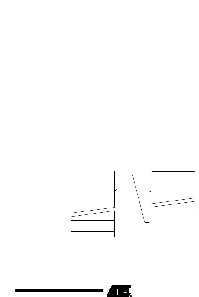
Since the Flash is organized in pages (see Table 22-6 on page 152), the Program Counter can be treated as having two different sections. One section, consisting of the least significant bits, is addressing the words within a page, while the most significant bits are addressing the pages. This is shown in Figure 21-1. Note that the Page Erase and Page Write operations are addressed independently. Therefore it is of major importance that the software addresses the same page in both the Page Erase and Page Write operation.
The LPM instruction uses the Z-pointer to store the address. Since this instruction addresses the
Flash byte-by-byte, also the LSB (bit Z0) of the Z-pointer is used.
Figure 21-1. Addressing the Flash During SPM(1)
BIT 15 |
|
|
|
ZPCMSB |
|
|
|
ZPAGEMSB 1 0 |
|
|||||||||
Z - REGISTER |
|
|
|
|
|
|
|
|
|
|
|
|
0 |
|
|
|
|
|
|
|
|
|
|
|
|
|
|
|
|
|
|
|
|
|
|
|
|
|
PROGRAM |
|
PCMSB |
|
|
|
PAGEMSB |
|
|
|
|
|||||||
|
|
|
PCPAGE |
PCWORD |
|
|
|
|
|
|||||||||
|
COUNTER |
|
|
|
|
|
||||||||||||
|
|
|
|
|
|
|
|
|
|
|
|
|
|
|||||
|
|
|
PAGE ADDRESS |
|
|
WORD ADDRESS |
|
|||||||||||
|
|
|
WITHIN THE FLASH |
|
|
WITHIN A PAGE |
|
|||||||||||
PROGRAM MEMORY |
|
|
|
|
|
|
|
|
|
PAGE |
PCWORD[PAGEMSB:0]: |
|||||||
|
|
|
|
|
|
|
|
|
|
|
|
|
|
|
|
|
|
|
|
PAGE |
|
|
|
|
|
|
|
|
|
|
|
|
INSTRUCTION WORD |
00 |
|||
|
|
|
|
|
|
|
|
|
|
|
|
|
|
|
||||
|
|
|
|
|
|
|
|
|
|
|
|
|
|
|
|
|
|
01 |
|
|
|
|
|
|
|
|
|
|
|
|
|
|
|
|
|
|
|
|
|
|
|
|
|
|
|
|
|
|
|
|
|
|
|
|
|
02 |
|
|
|
|
|
|
|
|
|
|
|
|
|
|
|
|
|
|
|
|
|
|
|
|
|
|
|
|
|
|
|
|
|
|
|
|
|
|
|
|
|
|
|
|
|
|
|
|
|
|
|
|
|
|
|
|
|
|
|
|
|
|
|
|
|
|
|
|
|
|
|
|
|
|
|
|
|
|
|
|
|
|
|
|
|
|
|
|
|
|
|
|
|
|
|
|
|
|
|
|
|
|
|
|
|
|
|
|
|
|
|
|
|
|
|
|
|
|
|
|
|
|
|
|
|
|
|
|
|
|
|
|
|
|
|
|
|
|
|
|
|
|
|
|
|
|
|
|
|
|
|
|
|
|
|
|
|
|
|
|
|
|
|
|
|
|
|
|
|
|
|
|
|
|
|
|
|
|
|
|
|
|
|
|
|
|
|
|
|
|
|
|
|
|
|
|
|
|
|
|
|
|
|
|
|
|
|
|
|
|
|
|
|
|
|
|
|
|
|
|
|
|
|
|
|
|
|
|
|
|
|
|
|
|
|
|
|
|
|
|
|
|
|
|
|
|
|
|
|
|
|
|
|
|
|
|
|
|
|
|
|
|
|
|
|
|
PAGEEND
Note: 1. The different variables used in Figure 21-1 are listed in Table 22-6 on page 152.
145
2586A–AVR–02/05

21.1.1Store Program Memory Control and Status Register – SPMCSR
The Store Program Memory Control and Status Register contains the control bits needed to control the Program memory operations.
Bit |
7 |
6 |
5 |
4 |
3 |
2 |
1 |
0 |
|
|
– |
– |
– |
CTPB |
RFLB |
PGWRT |
PGERS |
SPMEN |
SPMCSR |
|
|
|
|
|
|
|
|
|
|
Read/Write |
R |
R |
R |
R/W |
R/W |
R/W |
R/W |
R/W |
|
Initial Value |
0 |
0 |
0 |
0 |
0 |
0 |
0 |
0 |
|
• Bits 7..5 – Res: Reserved Bits
These bits are reserved bits in the ATtiny25/45/85 and always read as zero.
• Bit 4 – CTPB: Clear Temporary Page Buffer
If the CTPB bit is written while filling the temporary page buffer, the temporary page buffer will be cleared and the data will be lost.
• Bit 3 – RFLB: Read Fuse and Lock Bits
An LPM instruction within three cycles after RFLB and SPMEN are set in the SPMCSR Register, will read either the Lock bits or the Fuse bits (depending on Z0 in the Z-pointer) into the destination register. See ”EEPROM Write Prevents Writing to SPMCSR” on page 146 for details.
• Bit 2 – PGWRT: Page Write
If this bit is written to one at the same time as SPMEN, the next SPM instruction within four clock cycles executes Page Write, with the data stored in the temporary buffer. The page address is taken from the high part of the Z-pointer. The data in R1 and R0 are ignored. The PGWRT bit will auto-clear upon completion of a Page Write, or if no SPM instruction is executed within four clock cycles. The CPU is halted during the entire Page Write operation.
• Bit 1 – PGERS: Page Erase
If this bit is written to one at the same time as SPMEN, the next SPM instruction within four clock cycles executes Page Erase. The page address is taken from the high part of the Z-pointer. The data in R1 and R0 are ignored. The PGERS bit will auto-clear upon completion of a Page Erase, or if no SPM instruction is executed within four clock cycles. The CPU is halted during the entire Page Write operation.
• Bit 0 – SPMEN: Store Program Memory Enable
This bit enables the SPM instruction for the next four clock cycles. If written to one together with either CTPB, RFLB, PGWRT, or PGERS, the following SPM instruction will have a special meaning, see description above. If only SPMEN is written, the following SPM instruction will store the value in R1:R0 in the temporary page buffer addressed by the Z-pointer. The LSB of the Z-pointer is ignored. The SPMEN bit will auto-clear upon completion of an SPM instruction, or if no SPM instruction is executed within four clock cycles. During Page Erase and Page Write, the SPMEN bit remains high until the operation is completed.
Writing any other combination than “10001”, “01001”, “00101”, “00011” or “00001” in the lower five bits will have no effect.
21.1.2EEPROM Write Prevents Writing to SPMCSR
Note that an EEPROM write operation will block all software programming to Flash. Reading the
Fuses and Lock bits from software will also be prevented during the EEPROM write operation. It
146 ATtiny25/45/85 
2586A–AVR–02/05

 ATtiny25/45/85
is recommended that the user checks the status bit (EEWE) in the EECR Register and verifies that the bit is cleared before writing to the SPMCSR Register.
21.1.3Reading the Fuse and Lock Bits from Software
It is possible to read both the Fuse and Lock bits from software. To read the Lock bits, load the Z-pointer with 0x0001 and set the RFLB and SPMEN bits in SPMCSR. When an LPM instruction is executed within three CPU cycles after the RFLB and SPMEN bits are set in SPMCSR, the value of the Lock bits will be loaded in the destination register. The RFLB and SPMEN bits will auto-clear upon completion of reading the Lock bits or if no LPM instruction is executed within three CPU cycles or no SPM instruction is executed within four CPU cycles. When RFLB and SPMEN are cleared, LPM will work as described in the Instruction set Manual.
Bit |
7 |
6 |
5 |
4 |
3 |
2 |
1 |
0 |
Rd |
– |
– |
– |
– |
– |
– |
LB2 |
LB1 |
|
|
|
|
|
|
|
|
|
The algorithm for reading the Fuse Low byte is similar to the one described above for reading the Lock bits. To read the Fuse Low byte, load the Z-pointer with 0x0000 and set the RFLB and SPMEN bits in SPMCSR. When an LPM instruction is executed within three cycles after the RFLB and SPMEN bits are set in the SPMCSR, the value of the Fuse Low byte (FLB) will be loaded in the destination register as shown below. Refer to Table 22-5 on page 151 for a detailed description and mapping of the Fuse Low byte.
Bit |
7 |
6 |
5 |
4 |
3 |
2 |
1 |
0 |
Rd |
FLB7 |
FLB6 |
FLB5 |
FLB4 |
FLB3 |
FLB2 |
FLB1 |
FLB0 |
|
|
|
|
|
|
|
|
|
Similarly, when reading the Fuse High byte, load 0x0003 in the Z-pointer. When an LPM instruction is executed within three cycles after the RFLB and SPMEN bits are set in the SPMCSR, the value of the Fuse High byte (FHB) will be loaded in the destination register as shown below. Refer to Table XXX on page XXX for detailed description and mapping of the Fuse High byte.
Bit |
7 |
6 |
5 |
4 |
3 |
2 |
1 |
0 |
|
Rd |
FHB7 |
FHB6 |
FHB5 |
FHB4 |
FHB3 |
FHB2 |
FHB1 |
FHB0 |
|
|
|
|
|
|
|
|
|
|
|
Fuse and Lock bits that are programmed, will be read as zero. Fuse and Lock bits that are unprogrammed, will be read as one.
21.1.4Preventing Flash Corruption
During periods of low VCC, the Flash program can be corrupted because the supply voltage is too low for the CPU and the Flash to operate properly. These issues are the same as for board level systems using the Flash, and the same design solutions should be applied.
A Flash program corruption can be caused by two situations when the voltage is too low. First, a regular write sequence to the Flash requires a minimum voltage to operate correctly. Secondly, the CPU itself can execute instructions incorrectly, if the supply voltage for executing instructions is too low.
Flash corruption can easily be avoided by following these design recommendations (one is sufficient):
1.Keep the AVR RESET active (low) during periods of insufficient power supply voltage. This can be done by enabling the internal Brown-out Detector (BOD) if the operating voltage matches the detection level. If not, an external low VCC reset protection circuit can be
147
2586A–AVR–02/05