

ATtiny25/45/85
12. 8-bit Timer/Counter0 with PWM
Timer/Counter0 is a general purpose 8-bit Timer/Counter module, with two independent Output Compare Units, and with PWM support. It allows accurate program execution timing (event management) and wave generation. The main features are:
•Two Independent Output Compare Units
•Double Buffered Output Compare Registers
•Clear Timer on Compare Match (Auto Reload)
•Glitch Free, Phase Correct Pulse Width Modulator (PWM)
•Variable PWM Period
•Frequency Generator
•Three Independent Interrupt Sources (TOV0, OCF0A, and OCF0B)
12.1Overview
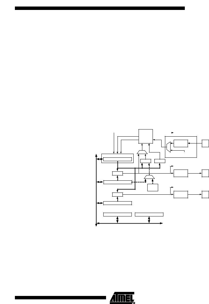
A simplified block diagram of the 8-bit Timer/Counter is shown in Figure 12-1. For the actual placement of I/O pins, refer to ”Pinout ATtiny25/45/85” on page 2. CPU accessible I/O Registers, including I/O bits and I/O pins, are shown in bold. The device-specific I/O Register and bit locations are listed in the ”8-bit Timer/Counter Register Description” on page 76.
Figure 12-1. 8-bit Timer/Counter Block Diagram
Count |
|
|
TOVn |
Clear |
|
|
(Int.Req.) |
|
|
Control Logic |
Clock Select |
|
|
|
|
Direction |
clkTn |
|
|
|
|
|
|
Edge |
Tn |
|
|
|
|
Detector |
|
|
|
|
|
|
|
|
|
TOP |
BOTTOM |
|
|
|
Timer/Counter |
|
|
( From Prescaler ) |
|
|
|
|
|
|
|
|
TCNTn |
= |
= 0 |
|
|
|
|
|
|
||
|
|
|
|
OCnA |
|
|
|
|
|
(Int.Req.) |
|
|
= |
|
|
Waveform |
OCnA |
|
|
|
Generation |
||
|
|
|
|
|
|
|
OCRnA |
|
|
|
|
|
|
|
Fixed |
OCnB |
|
|
|
|
TOP |
|
|
|
|
|
(Int.Req.) |
|
|
BUS |
|
|
Value |
|
|
= |
|
|
|
||
|
|
Waveform |
OCnB |
||
|
|
|
|
|
|
DATA |
|
|
|
Generation |
|
OCRnB |
|
|
|
|
|
|
|
|
|
|
|
|
TCCRnA |
TCCRnB |
|
|
|
12.1.1Registers
The Timer/Counter (TCNT0) and Output Compare Registers (OCR0A and OCR0B) are 8-bit registers. Interrupt request (abbreviated to Int.Req. in the figure) signals are all visible in the Timer Interrupt Flag Register (TIFR). All interrupts are individually masked with the Timer Interrupt Mask Register (TIMSK). TIFR and TIMSK are not shown in the figure.
The Timer/Counter can be clocked internally, via the prescaler, or by an external clock source on the T0 pin. The Clock Select logic block controls which clock source and edge the Timer/Counter uses to increment (or decrement) its value. The Timer/Counter is inactive when no clock source is selected. The output from the Clock Select logic is referred to as the timer clock (clkT0).
65
2586A–AVR–02/05