

ATtiny25/45/85
15. 8-bit Timer/Counter1 in ATtiny15 Mode
The ATtiny15 compatibility mode is selected by writing the code “0011” to the CKSEL fuses (if any other code is written, the Timer/Counter1 is working in normal mode). When selected the ATtiny15 compatibility mode provides an ATtiny15 backward compatible prescaler and Timer/Counter. Furthermore, the clocking system has same clock frequencies as in ATtiny15.
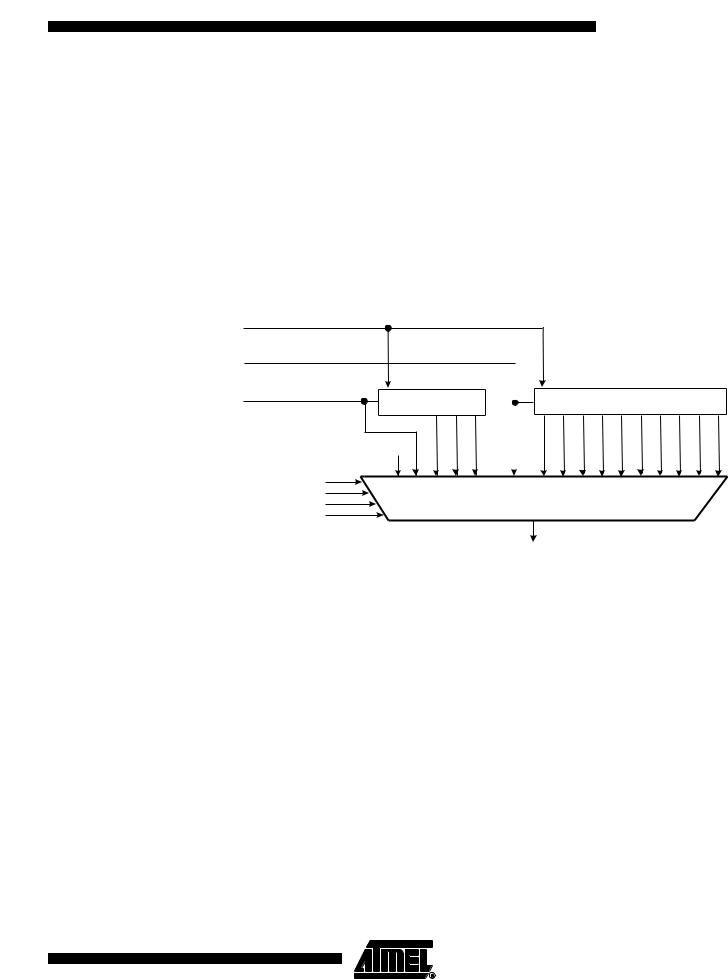
15.1Timer/Counter1 Prescaler
Figure 15-1 shows an ATtiny15 compatible prescaler. It has two prescaler units, the 3-bit prescaler for the the system clock (CK) and the 10-bit prescaler for the fast peripheral clock (PCK). The clocking system of the Timer/Counter1 is always synchronous in the ATtiny15 compatibility mode, because the same RC Oscillator is used as a PLL clock source (generates the input clock for the prescaler) and the AVR core.
Figure 15-1. |
Timer/Counter1 Prescaler |
|
|
|
|
|
|
|
|
|
|
|
|
|
|||
PSR1 |
|
|
|
|
|
|
|
|
|
|
|
|
|
|
|
|
|
CK (1.6 MHz) |
|
|
|
|
|
|
|
|
|
|
|
|
|
|
|
|
|
PCK (25.6 MHz) |
CLEAR |
|
|
|
|
CLEAR |
|
|
|
|
|
|
|
|
|||
|
|
3-BIT T/C PRESCALER |
|
|
|
|
10-BIT T/C PRESCALER |
|
|
||||||||
|
|
0 |
PCK |
PCK/2 |
PCK/4 |
PCK/8 |
CK |
CK/2 |
CK/4 |
CK/8 |
CK/16 |
CK/32 |
CK/64 |
CK/128 |
CK/256 |
CK/512 |
CK/1024 |
|
|
|
|||||||||||||||
|
CS10 |
|
|
|
|
|
|
|
|
|
|
|
|
|
|
|
|
|
CS11 |
|
|
|
|
|
|
|
|
|
|
|
|
|
|
|
|
|
CS12 |
|
|
|
|
|
|
|
|
|
|
|
|
|
|
|
|
|
CS13 |
|
|
|
|
|
|
|
|
|
|
|
|
|
|
|
|
TIMER/COUNTER1 COUNT ENABLE
The same clock selections as in ATtiny15 can be chosen for Timer/Counter1 from the output multiplexer, because the frequency of the fast peripheral clock is 25.6 MHz and the prescaler is similar in the ATtiny15 compatibility mode. The clock selections are PCK, PCK/2, PCK/4, PCK/8, CK, CK/2, CK/4, CK/8, CK/16, CK/32, CK/64, CK/128, CK/256, CK/512, CK/1024 and stop.
15.2Timer/Counter1
Figure 15-2 shows Timer/Counter 1 synchronization register block diagram and synchronization delays in between registers. Note that all clock gating details are not shown in the figure. The Timer/Counter1 register values go through the internal synchronization registers, which cause the input synchronization delay, before affecting the counter operation. The registers TCCR1, GTCCR, OCR1A and OCR1C can be read back right after writing the register. The read back values are delayed for the Timer/Counter1 (TCNT1) register and flags (OCF1A and TOV1), because of the input and output synchronization.
The Timer/Counter1 features a high resolution and a high accuracy usage with the lower prescaling opportunities. It can also support an accurate, high speed, 8-bit Pulse Width Modulator (PWM) using clock speeds up to 25.6 MHz. In this mode, Timer/Counter1 and the Output Compare Registers serve as a stand-alone PWM. Refer to page 104 for a detailed description on this function. Similarly, the high prescaling opportunities make this unit useful for lower speed functions or exact timing functions with infrequent actions.
97
2586A–AVR–02/05
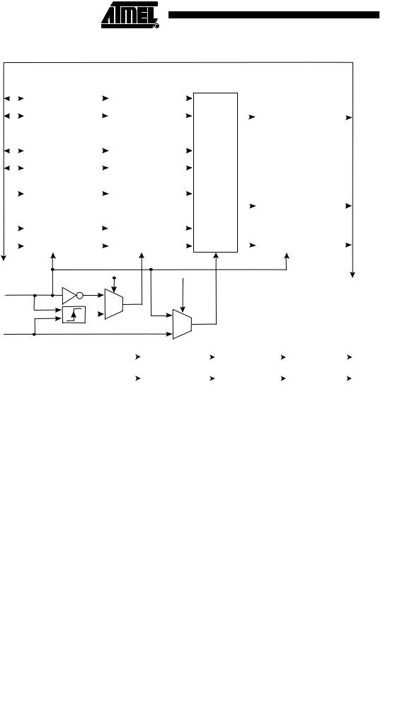
Figure 15-2. Timer/Counter 1 Synchronization Register Block Diagram.
|
|
|
|
|
|
|
|
|
|
|
|
|
|
|
|
|
8-BIT DATABUS |
|
|
|
|
|
|
||||
|
|
|
|
IO-registers |
|
|
|
|
Input synchronization |
|
|
Timer/Counter1 |
Output synchronization |
|
|||||||||||||
|
|
|
|
|
|
|
|
|
|
registers |
|
|
|
|
|
|
|
|
registers |
|
|
|
|||||
|
|
|
|
OCR1A |
|
|
|
|
|
OCR1A_SI |
|
|
|
|
|
|
|
|
|
|
|
|
TCNT1 |
|
|||
|
|
|
|
|
|
|
|
|
|
|
|
|
|
|
|
|
|
|
|
|
|
||||||
|
|
|
|
|
|
|
|
|
|
|
|
|
|
|
|
|
|
|
|
|
|
|
|
|
|
|
|
|
|
|
|
|
|
|
|
|
|
|
|
|
|
|
|
|
|
|
|
|
|
|
|
|
|
|
|
|
|
|
|
OCR1C |
|
|
|
|
|
OCR1C_SI |
|
|
|
|
|
|
|
|
|
TCNT_SO |
|
||||||
|
|
|
|
|
|
|
|
|
|
|
|
|
|
|
|
|
|
|
|
||||||||
|
|
|
|
|
|
|
|
|
|
|
|
|
|
|
|
|
|
|
|
|
|
|
|
|
|
|
|
|
|
|
|
|
|
|
|
|
|
|
|
|
|
|
|
|
|
|
|
|
|
|
|
|
|
|
|
|
|
|
|
TCCR1 |
|
|
|
|
|
TCCR1_SI |
|
|
|
|
|
|
|
|
|
|
|
|
|
|
|||
|
|
|
|
|
|
|
|
|
|
|
|
|
|
|
|
|
|
|
|
|
|
|
|||||
|
|
|
|
|
|
|
|
|
|
|
|
|
|
|
|
|
|
|
|
|
|
|
|
|
|
|
|
|
|
|
|
|
|
|
|
|
|
|
|
|
|
|
|
|
|
|
|
|
|
|
|
|
|
|
|
|
|
|
|
GTCCR |
|
|
|
|
|
GTCCR_SI |
|
|
|
|
TCNT1 |
|
|
|
|
|
|
||||||
|
|
|
|
|
|
|
|
|
|
|
|
|
|
|
|
|
|
|
|||||||||
|
|
|
|
|
|
|
|
|
|
|
|
|
|
|
|
|
|
|
|
|
|
|
|
||||
|
|
|
|
|
|
|
|
|
|
|
|
|
|
|
|
|
|
|
|
|
|
|
|
|
|
|
|
|
|
|
|
TCNT1 |
|
|
|
|
|
TCNT1_SI |
|
|
|
|
|
|
|
|
|
|
|
|
OCF1A |
|
|||
|
|
|
|
|
|
|
|
|
|
|
|
|
|
|
|
|
|
|
|
|
|
||||||
|
|
|
|
|
|
|
|
|
|
|
|
|
|
|
|
|
|
|
|
|
|
|
|
|
|
|
|
|
|
|
|
|
|
|
|
|
|
|
|
|
|
|
|
|
|
|
|
|
|
|
OCF1A_SO |
|
|
||
|
|
|
|
|
|
|
|
|
|
|
|
|
|
|
|
|
|
|
|
|
|
|
|
|
|
|
|
|
|
|
|
|
|
|
|
|
|
|
|
|
|
|
|
|
|
|
|
|
|
|
|
|
|
|
|
|
|
|
|
OCF1A |
|
|
|
|
|
OCF1A_SI |
|
|
|
|
|
|
|
|
|
|
|
|
TOV1 |
|
|||
|
|
|
|
|
|
|
|
|
|
|
|
|
|
|
|
|
|
|
|
|
|
||||||
|
|
|
|
|
|
|
|
|
|
|
|
|
|
|
|
|
|
|
|
|
|
|
|
|
|
|
|
|
|
|
|
|
|
|
|
|
|
|
|
|
|
|
|
|
|
|
|
|
|
|
|
|
|
|
|
|
|
|
|
TOV1 |
|
|
|
|
|
TOV1_SI |
|
|
|
|
|
|
|
|
|
TOV1_SO |
|
|
|||||
|
|
|
|
|
|
|
|
|
|
|
|
|
|
|
|
|
|
|
|
|
|
|
|
|
|||
PCKE |
|
|
|
|
|
|
|
|
|
|
|
|
|
|
|
|
|
|
|
|
|
|
|||||
CK |
|
|
|
|
S |
|
|
|
|
|
|
|
|
|
|
|
|
|
|
||||||||
|
|
|
|
|
|
|
|
|
|
|
|
|
|
|
|
|
|
||||||||||
|
|
|
|
|
|
|
|
|
|
|
|
|
|
|
|
|
|
|
|
|
|
|
|
||||
PCK |
|
|
|
|
A |
|
S |
|
|
|
|
|
|
|
|
|
|
||||||||||
|
|
|
|
|
|
|
|
|
|
|
|
|
|
|
|
|
|
|
|||||||||
|
|
|
|
|
|
|
|
|
A |
|
|
|
|
|
|
|
|
|
|
||||||||
SYNC |
|
1/2 CK Delay |
|
1CK Delay |
|
|
1/2 CK Delay |
No Delay |
|
||||||||||||||||||
MODE |
|
|
|
|
|
|
|
|
|
|
|
|
|
|
|
|
|
|
|
|
|
|
|
||||
ASYNC |
|
~1/2 CK Delay |
|
1PCK Delay |
|
|
1/2PCK - 1CK Delay |
No Delay |
|
||||||||||||||||||
MODE |
|
|
|
|
|
|
|
|
|
|
|
|
|
|
|
|
|
|
|
|
|
|
|
||||
|
|
|
|
|
|
|
|
|
|
|
|
|
|
|
|
|
|
|
|
|
|
|
|
|
|
|
|
Timer/Counter1 and the prescaler allow running the CPU from any clock source while the prescaler is operating on the fast 25.6 MHz PCK clock in the asynchronous mode.
The following Figure 15-3 shows the block diagram for Timer/Counter1.
98 ATtiny25/45/85 
2586A–AVR–02/05

ATtiny25/45/85
Figure 15-3. Timer/Counter1 Block Diagram
T/C1 OVER- T/C1 COMPARE |
OC1A |
FLOW IRQ MATCH A IRQ |
(PB1) |
OCIE1A |
TOIE1 TOIE0 |
OCF1A |
TOV1 TOV0 |
|
|
|
|
|
TIMER INT. MASK |
TIMER INT. FLAG |
|
|
T/C CONTROL |
GLOBAL T/C CONTROL |
|
REGISTER (TIMSK) |
REGISTER (TIFR) |
|
REGISTER 1 (TCCR1) |
REGISTER 2 (GTCCR) |
|||
|
|
OCF1A |
TOV1 |
CTC1 |
PWM1A |
COM1A1 COM1A0 CS13 CS12 CS11 CS10 |
FOC1A PSR1 |
TIMER/COUNTER1 |
|
|
|
|
|
|
|
|
TIMER/COUNTER1 |
T/C CLEAR |
|
|
|
T/C1 CONTROL |
CK |
|
(TCNT1) |
|
|
|
|
LOGIC |
PCK |
|
|
|
|
|
|
||
|
|
|
|
|
|
|
|
8-BIT COMPARATOR |
8-BIT COMPARATOR |
|
|
|
|
||
|
T/C1 OUTPUT |
T/C1 OUTPUT |
|
|
|
|
|
COMPARE REGISTER |
COMPARE REGISTER |
|
|
|
|
||
|
(OCR1A) |
|
(OCR1C) |
|
|
|
|
8-BIT DATABUS |
|
|
|
|
|
|
|
Two status flags (overflow and compare match) are found in the Timer/Counter Interrupt Flag Register - TIFR. Control signals are found in the Timer/Counter Control Registers TCCR1 and GTCCR. The interrupt enable/disable settings are found in the Timer/Counter Interrupt Mask Register - TIMSK.
The Timer/Counter1 contains two Output Compare Registers, OCR1A and OCR1C as the data source to be compared with the Timer/Counter1 contents. In normal mode the Output Compare functions are operational with OCR1A only. OCR1A determines action on the OC1A pin (PB1), and it can generate Timer1 OC1A interrupt in normal mode and in PWM mode. OCR1C holds the Timer/Counter maximum value, i.e. the clear on compare match value. In the normal mode an overflow interrupt (TOV1) is generated when Timer/Counter1 counts from $FF to $00, while in the PWM mode the overflow interrupt is generated when the Timer/Counter1 counts either from $FF to $00 or from OCR1C to $00.
In PWM mode, OCR1A provides the data values against which the Timer Counter value is compared. Upon compare match the PWM outputs (OC1A) is generated. In PWM mode, the Timer Counter counts up to the value specified in the output compare register OCR1C and starts again from $00. This feature allows limiting the counter “full” value to a specified value, lower than $FF. Together with the many prescaler options, flexible PWM frequency selection is provided. Table 14-6 lists clock selection and OCR1C values to obtain PWM frequencies from 20 kHz to 250 kHz in 10 kHz steps and from 250 kHz to 500 kHz in 50 kHz steps. Higher PWM frequencies can be obtained at the expense of resolution.
99
2586A–AVR–02/05

15.2.1Timer/Counter1 Control Register - TCCR1
Bit |
7 |
6 |
5 |
4 |
3 |
2 |
1 |
0 |
|
$30 ($50) |
CTC1 |
PWM1A |
COM1A1 |
COM1A0 |
CS13 |
CS12 |
CS11 |
CS10 |
TCCR1A |
|
|
|
|
|
|
|
|
|
|
Read/Write |
R/W |
R/W |
R/W |
R/W |
R/W |
R/W |
R/W |
R/W |
|
Initial value |
0 |
0 |
0 |
0 |
0 |
0 |
0 |
0 |
|
• Bit 7- CTC1 : Clear Timer/Counter on Compare Match
When the CTC1 control bit is set (one), Timer/Counter1 is reset to $00 in the CPU clock cycle after a compare match with OCR1A register. If the control bit is cleared, Timer/Counter1 continues counting and is unaffected by a compare match.
• Bit 6- PWM1A: Pulse Width Modulator A Enable
When set (one) this bit enables PWM mode based on comparator OCR1A in Timer/Counter1 and the counter value is reset to $00 in the CPU clock cycle after a compare match with OCR1C register value.
• Bits 5,4 - COM1A1, COM1A0: Comparator A Output Mode, Bits 1 and 0
The COM1A1 and COM1A0 control bits determine any output pin action following a compare match with compare register A in Timer/Counter1. Output pin actions affect pin PB1 (OC1A). Since this is an alternative function to an I/O port, the corresponding direction control bit must be set (one) in order to control an output pin.
Table 15-1. |
Comparator A Mode Select |
|
COM1A1 |
COM1A0 |
Description |
|
|
|
0 |
0 |
Timer/Counter Comparator A disconnected from output pin OC1A. |
|
|
|
0 |
1 |
Toggle the OC1A output line. |
|
|
|
1 |
0 |
Clear the OC1A output line. |
|
|
|
1 |
1 |
Set the OC1A output line |
|
|
|
In PWM mode, these bits have different functions. Refer to Table 15-3 on page 104 for a detailed description.
• Bits 3 .. 0 - CS13, CS12, CS11, CS10: Clock Select Bits 3, 2, 1, and 0
The Clock Select bits 3, 2, 1, and 0 define the prescaling source of Timer/Counter1.
Table 15-2. Timer/Counter1 Prescale Select
CS13 |
CS12 |
CS11 |
CS10 |
T/C1 Clock |
|
|
|
|
|
0 |
0 |
0 |
0 |
T/C1 stopped |
|
|
|
|
|
0 |
0 |
0 |
1 |
PCK |
|
|
|
|
|
0 |
0 |
1 |
0 |
PCK/2 |
|
|
|
|
|
0 |
0 |
1 |
1 |
PCK/4 |
|
|
|
|
|
0 |
1 |
0 |
0 |
PCK/8 |
|
|
|
|
|
0 |
1 |
0 |
1 |
CK |
|
|
|
|
|
0 |
1 |
1 |
0 |
CK/2 |
|
|
|
|
|
0 |
1 |
1 |
1 |
CK/4 |
|
|
|
|
|
100 ATtiny25/45/85 
2586A–AVR–02/05