

 ATtiny25/45/85
an interrupt when the transfer is complete. Note that when an external clock source is selected the counter counts both clock edges. In this case the counter counts the number of edges, and not the number of bits. The clock can be selected from three different sources: The USCK pin, Timer/Counter0 Compare Match or from software.
The Two-wire clock control unit can generate an interrupt when a start condition is detected on the Two-wire bus. It can also generate wait states by holding the clock pin low after a start condition is detected, or after the counter overflows.
17.2Functional Descriptions
17.2.1Three-wire Mode
The USI Three-wire mode is compliant to the Serial Peripheral Interface (SPI) mode 0 and 1, but does not have the slave select (SS) pin functionality. However, this feature can be implemented in software if necessary. Pin names used by this mode are: DI, DO, and USCK.
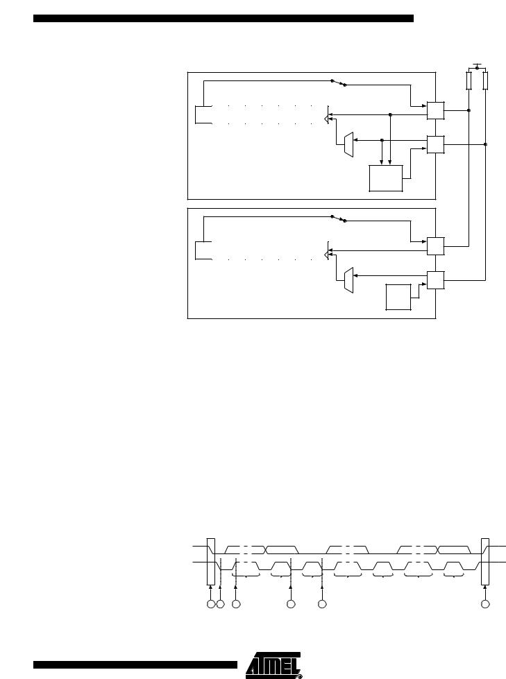
Figure 17-2. Three-wire Mode Operation, Simplified Diagram |
|
|||||||
|
|
|
|
|
|
|
|
DO |
Bit7 |
Bit6 |
Bit5 |
Bit4 |
Bit3 |
Bit2 |
Bit1 |
Bit0 |
DI |
|
||||||||
|
|
|
|
|
|
|
|
USCK |
SLAVE |
|
|
|
|
|
|
|
|
|
|
|
|
|
|
|
|
DO |
Bit7 |
Bit6 |
Bit5 |
Bit4 |
Bit3 |
Bit2 |
Bit1 |
Bit0 |
DI |
|
||||||||
|
|
|
|
|
|
|
|
USCK |
|
|
|
|
|
|
|
|
PORTxn |
MASTER |
|
|
|
|
|
|
|
|
Figure 17-2 shows two USI units operating in Three-wire mode, one as Master and one as Slave. The two Shift Registers are interconnected in such way that after eight USCK clocks, the data in each register are interchanged. The same clock also increments the USI’s 4-bit counter. The Counter Overflow (interrupt) Flag, or USIOIF, can therefore be used to determine when a transfer is completed. The clock is generated by the Master device software by toggling the USCK pin via the PORT Register or by writing a one to the USITC bit in USICR.
111
2586A–AVR–02/05
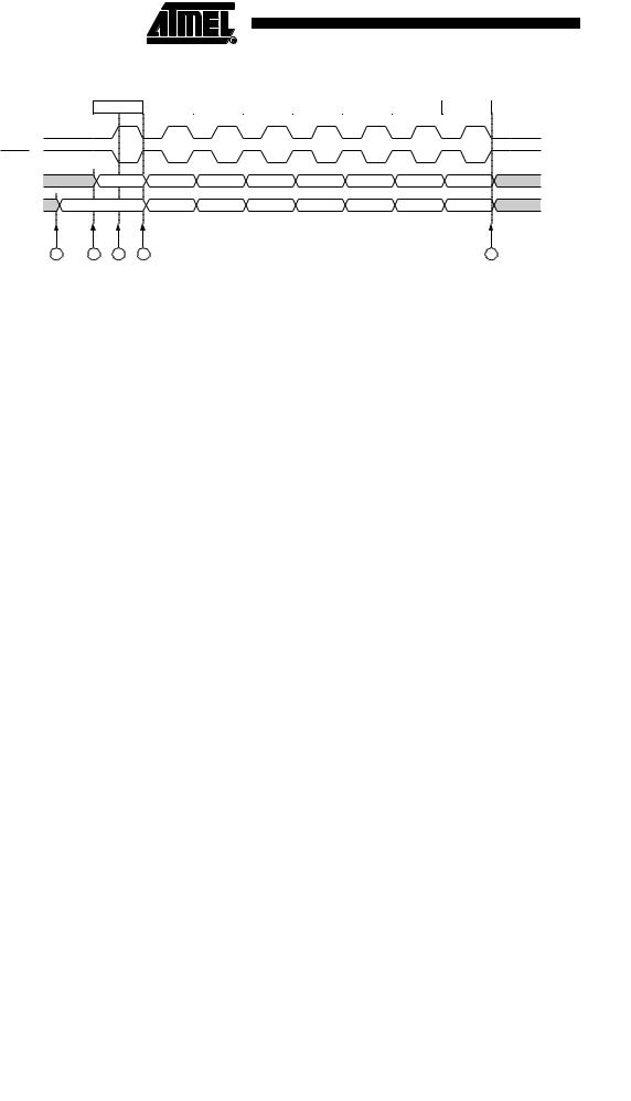
Figure 17-3. Three-wire Mode, Timing Diagram
CYCLE ( Reference ) |
1 |
2 |
3 |
4 |
5 |
6 |
7 |
8 |
USCK |
|
|
|
|
|
|
|
|
USCK |
|
|
|
|
|
|
|
|
DO |
MSB |
6 |
5 |
4 |
3 |
2 |
1 |
LSB |
DI |
MSB |
6 |
5 |
4 |
3 |
2 |
1 |
LSB |
A |
B C |
D |
|
|
|
|
|
E |
The Three-wire mode timing is shown in Figure 17-3. At the top of the figure is a USCK cycle reference. One bit is shifted into the USI Shift Register (USIDR) for each of these cycles. The USCK timing is shown for both external clock modes. In External Clock mode 0 (USICS0 = 0), DI is sampled at positive edges, and DO is changed (Data Register is shifted by one) at negative edges. External Clock mode 1 (USICS0 = 1) uses the opposite edges versus mode 0, i.e., samples data at negative and changes the output at positive edges. The USI clock modes corresponds to the SPI data mode 0 and 1.
Referring to the timing diagram (Figure 17-3.), a bus transfer involves the following steps:
1.The Slave device and Master device sets up its data output and, depending on the protocol used, enables its output driver (mark A and B). The output is set up by writing the data to be transmitted to the Serial Data Register. Enabling of the output is done by setting the corresponding bit in the port Data Direction Register. Note that point A and B does not have any specific order, but both must be at least one half USCK cycle before point C where the data is sampled. This must be done to ensure that the data setup requirement is satisfied. The 4-bit counter is reset to zero.
2.The Master generates a clock pulse by software toggling the USCK line twice (C and D). The bit value on the slave and master’s data input (DI) pin is sampled by the USI on the first edge (C), and the data output is changed on the opposite edge (D). The 4-bit counter will count both edges.
3.Step 2. is repeated eight times for a complete register (byte) transfer.
4.After eight clock pulses (i.e., 16 clock edges) the counter will overflow and indicate that the transfer is completed. The data bytes transferred must now be processed before a new transfer can be initiated. The overflow interrupt will wake up the processor if it is set to Idle mode. Depending of the protocol used the slave device can now set its output to high impedance.
17.2.2SPI Master Operation Example
The following code demonstrates how to use the USI module as a SPI Master:
SPITransfer:
sts |
USIDR,r16 |
ldi |
r16,(1<<USIOIF) |
sts |
USISR,r16 |
ldi |
r16,(1<<USIWM0)|(1<<USICS1)|(1<<USICLK)|(1<<USITC) |
SPITransfer_loop: |
|
sts |
USICR,r16 |
lds |
r16, USISR |
sbrs |
r16, USIOIF |
112 ATtiny25/45/85 
2586A–AVR–02/05

ATtiny25/45/85
rjmp SPITransfer_loop
lds r16,USIDR
ret
The code is size optimized using only eight instructions (+ ret). The code example assumes that the DO and USCK pins are enabled as output in the DDRE Register. The value stored in register r16 prior to the function is called is transferred to the Slave device, and when the transfer is completed the data received from the Slave is stored back into the r16 Register.
The second and third instructions clears the USI Counter Overflow Flag and the USI counter value. The fourth and fifth instruction set Three-wire mode, positive edge Shift Register clock, count at USITC strobe, and toggle USCK. The loop is repeated 16 times.
The following code demonstrates how to use the USI module as a SPI Master with maximum speed (fsck = fck/4):
SPITransfer_Fast:
sts |
USIDR,r16 |
ldi |
r16,(1<<USIWM0)|(0<<USICS0)|(1<<USITC) |
ldi |
r17,(1<<USIWM0)|(0<<USICS0)|(1<<USITC)|(1<<USICLK) |
sts |
USICR,r16 ; MSB |
sts |
USICR,r17 |
sts |
USICR,r16 |
sts |
USICR,r17 |
sts |
USICR,r16 |
sts |
USICR,r17 |
sts |
USICR,r16 |
sts |
USICR,r17 |
sts |
USICR,r16 |
sts |
USICR,r17 |
sts |
USICR,r16 |
sts |
USICR,r17 |
sts |
USICR,r16 |
sts |
USICR,r17 |
sts |
USICR,r16 ; LSB |
sts |
USICR,r17 |
lds |
r16,USIDR |
ret
113
2586A–AVR–02/05

17.2.3SPI Slave Operation Example
The following code demonstrates how to use the USI module as a SPI Slave:
init:
ldi r16,(1<<USIWM0)|(1<<USICS1) sts USICR,r16
...
SlaveSPITransfer:
sts |
USIDR,r16 |
ldi |
r16,(1<<USIOIF) |
sts |
USISR,r16 |
SlaveSPITransfer_loop: |
|
lds |
r16, USISR |
sbrs |
r16, USIOIF |
rjmp |
SlaveSPITransfer_loop |
lds |
r16,USIDR |
ret |
|
The code is size optimized using only eight instructions (+ ret). The code example assumes that the DO is configured as output and USCK pin is configured as input in the DDR Register. The value stored in register r16 prior to the function is called is transferred to the master device, and when the transfer is completed the data received from the Master is stored back into the r16 Register.
Note that the first two instructions is for initialization only and needs only to be executed once.These instructions sets Three-wire mode and positive edge Shift Register clock. The loop is repeated until the USI Counter Overflow Flag is set.
17.2.4Two-wire Mode
The USI Two-wire mode is compliant to the Inter IC (TWI) bus protocol, but without slew rate limiting on outputs and input noise filtering. Pin names used by this mode are SCL and SDA.
114 ATtiny25/45/85 
2586A–AVR–02/05
ATtiny25/45/85
Figure 17-4. Two-wire Mode Operation, Simplified Diagram
VCC
Bit7 Bit6 Bit5 Bit4 Bit3 Bit2 Bit1 Bit0 |
SDA |
|
|
|
SCL |
|
HOLD |
|
SCL |
|
Two-wire Clock |
|
Control Unit |
SLAVE |
|
|
|
|
|
|
|
|
Bit7 |
Bit6 |
Bit5 |
Bit4 |
Bit3 |
Bit2 |
Bit1 |
Bit0 |
SDA |
|
||||||||
|
|
|
|
|
|
|
|
SCL |
|
|
|
|
|
|
|
|
PORTxn |
MASTER |
|
|
|
|
|
|
|
|
Figure 17-4 shows two USI units operating in Two-wire mode, one as Master and one as Slave. It is only the physical layer that is shown since the system operation is highly dependent of the communication scheme used. The main differences between the Master and Slave operation at this level, is the serial clock generation which is always done by the Master, and only the Slave uses the clock control unit. Clock generation must be implemented in software, but the shift operation is done automatically by both devices. Note that only clocking on negative edge for shifting data is of practical use in this mode. The slave can insert wait states at start or end of transfer by forcing the SCL clock low. This means that the Master must always check if the SCL line was actually released after it has generated a positive edge.
Since the clock also increments the counter, a counter overflow can be used to indicate that the transfer is completed. The clock is generated by the master by toggling the USCK pin via the PORT Register.
The data direction is not given by the physical layer. A protocol, like the one used by the TWIbus, must be implemented to control the data flow.
Figure 17-5. Two-wire Mode, Typical Timing Diagram
SDA |
|
|
|
|
|
|
|
|
SCL |
1 - 7 |
8 |
9 |
1 - 8 |
9 |
1 - 8 |
9 |
|
S |
ADDRESS |
R/W |
ACK |
DATA |
ACK |
DATA |
ACK |
P |
A B |
C |
|
D |
E |
|
|
|
F |
Referring to the timing diagram (Figure 17-5.), a bus transfer involves the following steps:
115
2586A–AVR–02/05