

|
|
|
|
|
|
|
|
ATtiny25/45/85 |
|
|
|
|
|
|
|
|
|
||
|
|
Table 15-2. |
Timer/Counter1 Prescale Select |
(Continued) |
|||||
|
|
|
|
||||||
|
|
|
|||||||
|
|
|
|
|
|
|
|
|
|
|
|
CS13 |
|
CS12 |
CS11 |
|
CS10 |
|
T/C1 Clock |
|
|
|
|
|
|
|
|
|
|
|
|
1 |
|
0 |
0 |
|
0 |
|
CK/8 |
|
|
|
|
|
|
|
|
|
|
|
|
1 |
|
0 |
0 |
|
1 |
|
CK/16 |
|
|
|
|
|
|
|
|
|
|
|
|
1 |
|
0 |
1 |
|
0 |
|
CK/32 |
|
|
|
|
|
|
|
|
|
|
|
|
1 |
|
0 |
1 |
|
1 |
|
CK/64 |
|
|
|
|
|
|
|
|
|
|
|
|
1 |
|
1 |
0 |
|
0 |
|
CK/128 |
|
|
|
|
|
|
|
|
|
|
|
|
1 |
|
1 |
0 |
|
1 |
|
CK/256 |
|
|
|
|
|
|
|
|
|
|
|
|
1 |
|
1 |
1 |
|
0 |
|
CK/512 |
|
|
|
|
|
|
|
|
|
|
|
|
1 |
|
1 |
1 |
|
1 |
|
CK/1024 |
|
|
|
|
|
|
|
|
|
|
The Stop condition provides a Timer Enable/Disable function.
15.2.2General Timer/Counter1 Control Register - GTCCR
Bit |
7 |
6 |
5 |
4 |
3 |
2 |
1 |
0 |
|
|
$2C ($4C) |
|
TSM |
PWM1B |
COM1B1 |
COM1B0 |
FOC1B |
FOC1A |
PSR1 |
PSR0 |
GTCCR |
Read/Write |
|
R/W |
R/W |
R/W |
R/W |
W |
W |
R/W |
R/W |
|
Initial value |
0 |
0 |
0 |
0 |
0 |
0 |
0 |
0 |
|
|
• Bit 2- FOC1A: Force Output Compare Match 1A
Writing a logical one to this bit forces a change in the compare match output pin PB1 (OC1A) according to the values already set in COM1A1 and COM1A0. If COM1A1 and COM1A0 written in the same cycle as FOC1A, the new settings will be used. The Force Output Compare bit can be used to change the output pin value regardless of the timer value. The automatic action programmed in COM1A1 and COM1A0 takes place as if a compare match had occurred, but no interrupt is generated. The FOC1A bit always reads as zero. FOC1A is not in use if PWM1A bit is set.
• Bit 1- PSR1 : Prescaler Reset Timer/Counter1
When this bit is set (one), the Timer/Counter prescaler (TCNT1 is unaffected) will be reset. The bit will be cleared by hardware after the operation is performed. Writing a zero to this bit will have no effect. This bit will always read as zero.
15.2.3Timer/Counter1 - TCNT1
Bit |
7 |
6 |
5 |
4 |
3 |
2 |
1 |
0 |
|
|
$2F ($4F) |
MSB |
|
|
|
|
|
|
LSB |
TCNT1 |
|
|
|
|
|
|
|
|
|
|
|
|
Read/Write |
R/W |
R/W |
R/W |
R/W |
R/W |
R/W |
R/W |
R/W |
|
|
Initial value |
0 |
0 |
0 |
0 |
0 |
0 |
0 |
0 |
|
|
This 8-bit register contains the value of Timer/Counter1.
Timer/Counter1 is realized as an up counter with read and write access. Due to synchronization of the CPU, Timer/Counter1 data written into Timer/Counter1 is delayed by one CPU clock cycle in synchronous mode and at most two CPU clock cycles for asynchronous mode.
101
2586A–AVR–02/05

15.2.4Timer/Counter1 Output Compare RegisterA - OCR1A
Bit |
7 |
6 |
5 |
4 |
3 |
2 |
1 |
0 |
|
$2E ($4E) |
MSB |
|
|
|
|
|
|
LSB |
OCR1A |
|
|
|
|
|
|
|
|
|
|
Read/Write |
R/W |
R/W |
R/W |
R/W |
R/W |
R/W |
R/W |
R/W |
|
Initial value |
0 |
0 |
0 |
0 |
0 |
0 |
0 |
0 |
|
The output compare register A is an 8-bit read/write register.
The Timer/Counter Output Compare Register A contains data to be continuously compared with Timer/Counter1. Actions on compare matches are specified in TCCR1. A compare match does only occur if Timer/Counter1 counts to the OCR1A value. A software write that sets TCNT1 and OCR1A to the same value does not generate a compare match.
A compare match will set the compare interrupt flag OCF1A after a synchronization delay following the compare event.
15.2.5Timer/Counter1 Output Compare Register C - OCR1C
Bit |
7 |
6 |
5 |
4 |
3 |
2 |
1 |
0 |
|
$2B ($4B) |
MSB |
|
|
|
|
|
|
LSB |
OCR1C |
|
|
|
|
|
|
|
|
|
|
Read/Write |
R/W |
R/W |
R/W |
R/W |
R/W |
R/W |
R/W |
R/W |
|
Initial value |
1 |
1 |
1 |
1 |
1 |
1 |
1 |
1 |
|
The Output Compare Register B - OCR1B from ATtiny15 is replaced with the output compare register C - OCR1C that is an 8-bit read/write register. This register has the same function as the Output Compare Register B in ATtiny15.
The Timer/Counter Output Compare Register C contains data to be continuously compared with Timer/Counter1. A compare match does only occur if Timer/Counter1 counts to the OCR1C value. A software write that sets TCNT1 and OCR1C to the same value does not generate a compare match. If the CTC1 bit in TCCR1 is set, a compare match will clear TCNT1.
15.2.6Timer/Counter1 Interrupt Mask Register - TIMSK
Bit |
7 |
6 |
5 |
4 |
3 |
2 |
1 |
0 |
|
$39 ($59) |
- |
OCIE1A |
OCIE1B |
OCIE0A |
OCIE0B |
TOIE1 |
TOIE0 |
- |
TIMSK |
Read/Write |
R |
R/W |
R/W |
R |
R |
R/W |
R/W |
R |
|
Initial value |
0 |
0 |
0 |
0 |
0 |
0 |
0 |
0 |
|
• Bit 7 - Res: Reserved Bit
This bit is a reserved bit in the ATtiny25/45/85 and always reads as zero.
• Bit 6 - OCIE1A: Timer/Counter1 Output Compare Interrupt Enable
When the OCIE1A bit is set (one) and the I-bit in the Status Register is set (one), the Timer/Counter1 Compare MatchA, interrupt is enabled. The corresponding interrupt at vector $003 is executed if a compare matchA occurs. The Compare Flag in Timer/Counter1 is set (one) in the Timer/Counter Interrupt Flag Register.
• Bit 2 - TOIE1: Timer/Counter1 Overflow Interrupt Enable
When the TOIE1 bit is set (one) and the I-bit in the Status Register is set (one), the Timer/Counter1 Overflow interrupt is enabled. The corresponding interrupt (at vector $004) is executed if an overflow in Timer/Counter1 occurs. The Overflow Flag (Timer1) is set (one) in the Timer/Counter Interrupt Flag Register - TIFR.
102 ATtiny25/45/85
2586A–AVR–02/05

ATtiny25/45/85
• Bit 0 - Res: Reserved Bit
This bit is a reserved bit in the ATtiny25/45/85 and always reads as zero.
15.2.7Timer/Counter Interrupt Flag Register - TIFR
Bit |
7 |
6 |
5 |
4 |
3 |
2 |
1 |
0 |
|
$38 ($58) |
- |
OCF1A |
OCF1B |
OCF0A |
OCF0B |
TOV1 |
TOV0 |
- |
TIFR |
Read/Write |
R |
R/W |
R/W |
R |
R |
R/W |
R/W |
R |
|
Initial value |
0 |
0 |
0 |
0 |
0 |
0 |
0 |
0 |
|
• Bit 7 - Res: Reserved Bit
This bit is a reserved bit in the ATtiny25/45/85 and always reads as zero.
• Bit 6 - OCF1A: Output Compare Flag 1A
The OCF1A bit is set (one) when compare match occurs between Timer/Counter1 and the data value in OCR1A - Output Compare Register 1A. OCF1A is cleared by hardware when executing the corresponding interrupt handling vector. Alternatively, OCF1A is cleared, after synchronization clock cycle, by writing a logic one to the flag. When the I-bit in SREG, OCIE1A, and OCF1A are set (one), the Timer/Counter1 A compare match interrupt is executed.
• Bit 2 - TOV1: Timer/Counter1 Overflow Flag
The bit TOV1 is set (one) when an overflow occurs in Timer/Counter1. TOV1 is cleared by hardware when executing the corresponding interrupt handling vector. Alternatively, TOV1 is cleared, after synchronization clock cycle, by writing a logical one to the flag. When the SREG I- bit, and TOIE1 (Timer/Counter1 Overflow Interrupt Enable), and TOV1 are set (one), the Timer/Counter1 Overflow interrupt is executed.
• Bit 0 - Res: Reserved Bit
This bit is a reserved bit in the ATtiny25/45/85 and always reads as zero.
15.2.8PLL Control and Status Register - PLLCSR
Bit |
7 |
6 |
5 |
4 |
3 |
2 |
1 |
0 |
|
$27 ($27) |
LSM |
- |
- |
- |
- |
PCKE |
PLLE |
PLOCK |
PLLCSR |
Read/Write |
R |
R |
R |
R |
R |
R/W |
R/W |
R |
|
Initial value |
0 |
0 |
0 |
0 |
0 |
0 |
0/1 |
0 |
|
• Bit 7.. 3- Res : Reserved Bits
These bits are reserved bits in the ATtiny25/45/85 and always read as zero.
• Bit 2- PCKE: PCK Enable
The bit PCKE is always set in the ATtiny15 compatibility mode.
• Bit 1- PLLE: PLL Enable
The PLL is always enabled in the ATtiny15 compatibility mode.
• Bit 0- PLOCK: PLL Lock Detector
When the PLOCK bit is set, the PLL is locked to the reference clock.
103
2586A–AVR–02/05
15.2.9Timer/Counter1 in PWM Mode
When the PWM mode is selected, Timer/Counter1 and the Output Compare Register A -
OCR1A form an 8-bit, free-running and glitch-free PWM generator with output on the
PB1(OC1A).
When the counter value match the content of OCR1A, the OC1A and output is set or cleared according to the COM1A1/COM1A0 bits in the Timer/Counter1 Control Register A - TCCR1, as shown in Table 15-3.
Timer/Counter1 acts as an up-counter, counting from $00 up to the value specified in the output compare register OCR1C, and starting from $00 up again. A compare match with OCR1C will set an overflow interrupt flag (TOV1) after a synchronization delay following the compare event.
Table 15-3. |
Compare Mode Select in PWM Mode |
|
COM1A1 |
COM1A0 |
Effect on Output Compare Pin |
|
|
|
0 |
0 |
OC1A not connected. |
|
|
|
0 |
1 |
OC1A not connected. |
|
|
|
1 |
0 |
OC1A cleared on compare match. Set when TCNT1 = $01. |
|
|
|
1 |
1 |
OC1A set on compare match. Cleared when TCNT1 = $01. |
|
|
|
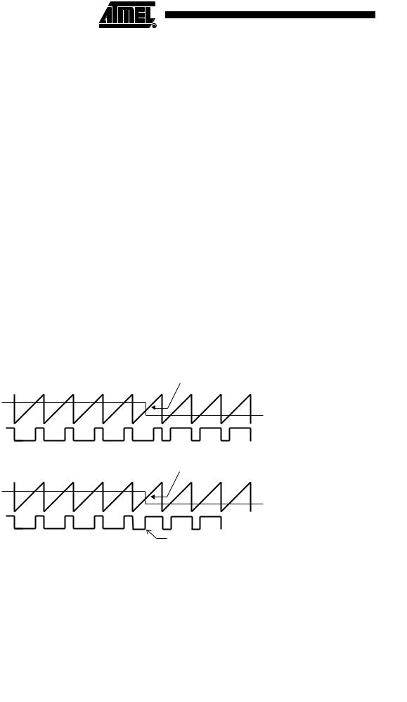
Note that in PWM mode, writing to the Output Compare Register OCR1A, the data value is first transferred to a temporary location. The value is latched into OCR1A when the Timer/Counter reaches OCR1C. This prevents the occurrence of odd-length PWM pulses (glitches) in the event of an unsynchronized OCR1A. See Figure 15-4 for an e xample.
Figure 15-4. Effects of Unsynchronized OCR Latching
Compare Value changes
Counter Value
Compare Value
PWM Output OC1A
Synchronized OC1A Latch
Compare Value changes
Counter Value
Compare Value
|
PWM Output OC1A |
Unsynchronized OC1A Latch |
Glitch |
During the time between the write and the latch operation, a read from OCR1A will read the contents of the temporary location. This means that the most recently written value always will read out of OCR1A.
104 ATtiny25/45/85 
2586A–AVR–02/05

ATtiny25/45/85
When OCR1A contains $00 or the top value, as specified in OCR1C register, the output PB1(OC1A) is held low or high according to the settings of COM1A1/COM1A0. This is shown in Table 15-4.
Table 15-4. PWM Outputs OCR1A = $00 or OCR1C
COM1A1 |
COM1A0 |
OCR1A |
Output OC1A |
|
|
|
|
0 |
1 |
$00 |
L |
|
|
|
|
0 |
1 |
OCR1C |
H |
|
|
|
|
1 |
0 |
$00 |
L |
|
|
|
|
1 |
0 |
OCR1C |
H |
|
|
|
|
1 |
1 |
$00 |
H |
|
|
|
|
1 |
1 |
OCR1C |
L |
|
|
|
|
In PWM mode, the Timer Overflow Flag - TOV1 is set when the TCNT1 counts to the OCR1C value and the TCNT1 is reset to $00. The Timer Overflow Interrupt1 is executed when TOV1 is set provided that Timer Overflow Interrupt and global interrupts are enabled. This also applies to the Timer Output Compare flags and interrupts.
The frequency of the PWM will be Timer Clock 1 Frequency divided by (OCR1C value + 1). See the following equation:
ffTCK1
=-----------------------------------
PWM (OCR1C + 1)
Resolution shows how many bit is required to express the value in the OCR1C register. It is calculated by following equation
ResolutionPWM = log2(OCR1C + 1).
105
2586A–AVR–02/05

Table 15-5. Timer/Counter1 Clock Prescale Select in the Asynchronous Mode
PWM Frequency |
Clock Selection |
CS13..CS10 |
OCR1C |
RESOLUTION |
|
|
|
|
|
20 kHz |
PCK/16 |
0101 |
199 |
7.6 |
|
|
|
|
|
30 kHz |
PCK/16 |
0101 |
132 |
7.1 |
|
|
|
|
|
40 kHz |
PCK/8 |
0100 |
199 |
7.6 |
|
|
|
|
|
50 kHz |
PCK/8 |
0100 |
159 |
7.3 |
|
|
|
|
|
60 kHz |
PCK/8 |
0100 |
132 |
7.1 |
|
|
|
|
|
70 kHz |
PCK/4 |
0011 |
228 |
7.8 |
|
|
|
|
|
80 kHz |
PCK/4 |
0011 |
199 |
7.6 |
|
|
|
|
|
90 kHz |
PCK/4 |
0011 |
177 |
7.5 |
|
|
|
|
|
100 kHz |
PCK/4 |
0011 |
159 |
7.3 |
|
|
|
|
|
110 kHz |
PCK/4 |
0011 |
144 |
7.2 |
|
|
|
|
|
120 kHz |
PCK/4 |
0011 |
132 |
7.1 |
|
|
|
|
|
130 kHz |
PCK/2 |
0010 |
245 |
7.9 |
|
|
|
|
|
140 kHz |
PCK/2 |
0010 |
228 |
7.8 |
|
|
|
|
|
150 kHz |
PCK/2 |
0010 |
212 |
7.7 |
|
|
|
|
|
160 kHz |
PCK/2 |
0010 |
199 |
7.6 |
|
|
|
|
|
170 kHz |
PCK/2 |
0010 |
187 |
7.6 |
|
|
|
|
|
180 kHz |
PCK/2 |
0010 |
177 |
7.5 |
|
|
|
|
|
190 kHz |
PCK/2 |
0010 |
167 |
7.4 |
|
|
|
|
|
200 kHz |
PCK/2 |
0010 |
159 |
7.3 |
|
|
|
|
|
250 kHz |
PCK |
0001 |
255 |
8.0 |
|
|
|
|
|
300 kHz |
PCK |
0001 |
212 |
7.7 |
|
|
|
|
|
350 kHz |
PCK |
0001 |
182 |
7.5 |
|
|
|
|
|
400 kHz |
PCK |
0001 |
159 |
7.3 |
|
|
|
|
|
450 kHz |
PCK |
0001 |
141 |
7.1 |
|
|
|
|
|
500 kHz |
PCK |
0001 |
127 |
7.0 |
|
|
|
|
|
106 ATtiny25/45/85 
2586A–AVR–02/05