

 ATtiny25/45/85
22.6Serial Downloading
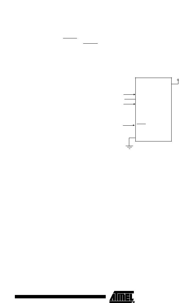
Both the Flash and EEPROM memory arrays can be programmed using the serial SPI bus while RESET is pulled to GND. The serial interface consists of pins SCK, MOSI (input) and MISO (output). After RESET is set low, the Programming Enable instruction needs to be executed first before program/erase operations can be executed. NOTE, in Table 22-8 on page 153, the pin mapping for SPI programming is listed. Not all parts use the SPI pins dedicated for the internal SPI interface.
Figure 22-1. Serial Programming and Verify(1)
+1.8 - 5.5V
VCC
MOSI
MISO 
SCK
RESET
GND
Notes: 1. If the device is clocked by the internal Oscillator, it is no need to connect a clock source to the CLKI pin.
Table 22-8. Pin Mapping Serial Programming
Symbol |
Pins |
I/O |
Description |
|
|
|
|
MOSI |
PB0 |
I |
Serial Data in |
|
|
|
|
MISO |
PB1 |
O |
Serial Data out |
|
|
|
|
SCK |
PB2 |
I |
Serial Clock |
|
|
|
|
When programming the EEPROM, an auto-erase cycle is built into the self-timed programming operation (in the Serial mode ONLY) and there is no need to first execute the Chip Erase instruction. The Chip Erase operation turns the content of every memory location in both the Program and EEPROM arrays into 0xFF.
Depending on CKSEL Fuses, a valid clock must be present. The minimum low and high periods for the serial clock (SCK) input are defined as follows:
Low: > 2 CPU clock cycles for fck < 12 MHz, 3 CPU clock cycles for fck >= 12 MHz
High: > 2 CPU clock cycles for fck < 12 MHz, 3 CPU clock cycles for fck >= 12 MHz
22.6.1Serial Programming Algorithm
When writing serial data to the ATtiny25/45/85, data is clocked on the rising edge of SCK.
When reading data from the ATtiny25/45/85, data is clocked on the falling edge of SCK. See Figure 22-2 and Figure 22-3 for timing details.
153
2586A–AVR–02/05

To program and verify the ATtiny25/45/85 in the Serial Programming mode, the following sequence is recommended (see four byte instruction formats in Table 22-10):
1.Power-up sequence:
Apply power between VCC and GND while RESET and SCK are set to “0”. In some systems, the programmer can not guarantee that SCK is held low during power-up. In this case, RESET must be given a positive pulse of at least two CPU clock cycles duration after SCK has been set to “0”.
2.Wait for at least 20 ms and enable serial programming by sending the Programming Enable serial instruction to pin MOSI.
3.The serial programming instructions will not work if the communication is out of synchronization. When in sync. the second byte (0x53), will echo back when issuing the third byte of the Programming Enable instruction. Whether the echo is correct or not, all four bytes of the instruction must be transmitted. If the 0x53 did not echo back, give RESET a positive pulse and issue a new Programming Enable command.
4.The Flash is programmed one page at a time. The memory page is loaded one byte at a time by supplying the 5 LSB of the address and data together with the Load Program memory Page instruction. To ensure correct loading of the page, the data low byte must be loaded before data high byte is applied for a given address. The Program memory Page is stored by loading the Write Program memory Page instruction with the 6 MSB of
the address. If polling (RDY/BSY) is not used, the user must wait at least tWD_FLASH before issuing the next page. (See Table 22-9.) Accessing the serial programming interface before the Flash write operation completes can result in incorrect programming.
5.A: The EEPROM array is programmed one byte at a time by supplying the address and data together with the appropriate Write instruction. An EEPROM memory location is first automatically erased before new data is written. If polling (RDY/BSY) is not used, the
user must wait at least tWD_EEPROM before issuing the next byte. (See Table 22-9.) In a chip erased device, no 0xFFs in the data file(s) need to be programmed.
B: The EEPROM array is programmed one page at a time. The Memory page is loaded one byte at a time by supplying the 2 LSB of the address and data together with the Load EEPROM Memory Page instruction. The EEPROM Memory Page is stored by loading the Write EEPROM Memory Page Instruction with the 6 MSB of the address. When using EEPROM page access only byte locations loaded with the Load EEPROM Memory Page instruction is altered. The remaining locations remain unchanged. If polling (RDY/BSY) is
not used, the used must wait at least tWD_EEPROM before issuing the next page (See Table 22-7). In a chip erased device, no 0xFF in the data file(s) need to be programmed.
6.Any memory location can be verified by using the Read instruction which returns the content at the selected address at serial output MISO.
7.At the end of the programming session, RESET can be set high to commence normal operation.
8.Power-off sequence (if needed): Set RESET to “1”.
Turn VCC power off.
154 ATtiny25/45/85 
2586A–AVR–02/05

|
|
|
|
|
ATtiny25/45/85 |
|
|
|
|
|
|
|
|
Table 22-9. |
|
|
|
|
|
Minimum Wait Delay Before Writing the Next Flash or EEPROM Location |
|||
|
|
||||
|
|
|
|
|
|
|
|
Symbol |
|
Minimum Wait Delay |
|
|
|
|
|
|
|
|
|
tWD_FLASH |
|
4.5 ms |
|
|
|
tWD_EEPROM |
|
4.0 ms |
|
|
|
tWD_ERASE |
|
4.0 ms |
|
|
|
tWD_FUSE |
|
4.5 ms |
|
Figure 22-2. Serial Programming Waveforms
SERIAL DATA INPUT |
MSB |
LSB |
(MOSI) |
|
|
SERIAL DATA OUTPUT |
MSB |
LSB |
(MISO) |
|
|
SERIAL CLOCK INPUT |
|
|
(SCK) |
|
|
SAMPLE |
|
|
155
2586A–AVR–02/05

Table 22-10. Serial Programming Instruction Set
|
|
Instruction Format |
|
|
|
|
||
|
|
|
|
|
|
|
||
Instruction |
Byte 1 |
Byte 2 |
Byte 3 |
Byte4 |
|
Operation |
||
|
|
|
|
|
|
|
|
|
Programming Enable |
1010 1100 |
0101 |
0011 |
xxxx xxxx |
xxxx xxxx |
|
Enable Serial Programming after |
|
|
|
|
|
|
|
|
|
|
|
|
|
|
|
|
RESET goes low. |
||
|
|
|
|
|
|
|
||
|
|
|
|
|
|
|
|
|
Chip Erase |
1010 1100 |
100x |
xxxx |
xxxx xxxx |
xxxx xxxx |
|
Chip Erase EEPROM and Flash. |
|
|
|
|
|
|
|
|
|
|
Read Program Memory |
0010 H000 |
0000 |
000a |
bbbb bbbb |
oooo oooo |
|
Read H (high or low) data o from |
|
|
|
|
|
|
|
Program memory at word address a:b. |
||
|
|
|
|
|
|
|
||
|
|
|
|
|
|
|
|
|
|
0100 H000 |
000x |
xxxx |
xxxb bbbb |
iiii iiii |
|
Write H (high or low) data i to Program |
|
|
|
|
|
|
|
|
memory page at word address b. Data |
|
Load Program Memory Page |
|
|
|
|
|
|
low byte must be loaded before Data |
|
|
|
|
|
|
|
|
high byte is applied within the same |
|
|
|
|
|
|
|
|
address. |
|
|
|
|
|
|
|
|
|
|
Write Program Memory Page |
0100 1100 |
0000 |
000a |
bbxx xxxx |
xxxx xxxx |
|
Write Program memory Page at |
|
|
|
|
|
|
|
address a:b. |
||
|
|
|
|
|
|
|
||
|
|
|
|
|
|
|
|
|
Read EEPROM Memory |
1010 0000 |
000x |
xxxx |
xxbb bbbb |
oooo oooo |
|
Read data o from EEPROM memory at |
|
|
|
|
|
|
|
address b. |
||
|
|
|
|
|
|
|
||
|
|
|
|
|
|
|
|
|
Write EEPROM Memory |
1100 0000 |
000x |
xxxx |
xxbb bbbb |
iiii iiii |
|
Write data i to EEPROM memory at |
|
|
|
|
|
|
|
address b. |
||
|
|
|
|
|
|
|
||
|
|
|
|
|
|
|
|
|
Load EEPROM Memory |
1100 0001 |
0000 |
0000 |
0000 00bb |
iiii iiii |
|
Load data i to EEPROM memory page |
|
Page (page access) |
|
|
|
|
|
|
buffer. After data is loaded, program |
|
|
|
|
|
|
|
EEPROM page. |
||
|
|
|
|
|
|
|
||
|
|
|
|
|
|
|
||
Write EEPROM Memory |
1100 0010 |
00xx xxxx |
xxbb bb00 |
xxxx xxxx |
|
Write EEPROM page at address b. |
||
Page (page access) |
|
|
|
|
|
|
|
|
|
0101 1000 |
0000 |
0000 |
xxxx xxxx |
xxoo oooo |
|
Read Lock bits. “0” = programmed, “1” |
|
Read Lock bits |
|
|
|
|
|
|
= unprogrammed. See Table 22-1 on |
|
|
|
|
|
|
|
|
page 149 for details. |
|
|
|
|
|
|
|
|
|
|
|
1010 1100 |
111x |
xxxx |
xxxx xxxx |
11ii iiii |
|
Write Lock bits. Set bits = “0” to |
|
Write Lock bits |
|
|
|
|
|
|
program Lock bits. See Table 22-1 on |
|
|
|
|
|
|
|
|
page 149 for details. |
|
|
|
|
|
|
|
|
|
|
Read Signature Byte |
0011 0000 |
000x |
xxxx |
xxxx xxbb |
oooo oooo |
|
Read Signature Byte o at address b. |
|
|
|
|
|
|
|
|
|
|
|
1010 1100 |
1010 |
0000 |
xxxx xxxx |
iiii iiii |
|
Set bits = “0” to program, “1” to |
|
Write Fuse bits |
|
|
|
|
|
|
unprogram. See Table 22-5 on page |
|
|
|
|
|
|
|
|
151 for details. |
|
|
|
|
|
|
|
|
|
|
|
1010 1100 |
1010 |
1000 |
xxxx xxxx |
iiii iiii |
|
Set bits = “0” to program, “1” to |
|
Write Fuse High bits |
|
|
|
|
|
|
unprogram. See Table 22-4 on page |
|
|
|
|
|
|
|
|
150 for details. |
|
|
|
|
|
|
|
|
|
|
|
1010 1100 |
1010 |
0100 |
xxxx xxxx |
xxxx xxxi |
|
Set bits = “0” to program, “1” to |
|
Write Extended Fuse Bits |
|
|
|
|
|
|
unprogram. See Table 22-3 on page |
|
|
|
|
|
|
|
|
150 for details. |
|
|
|
|
|
|
|
|
|
|
|
0101 0000 |
0000 |
0000 |
xxxx xxxx |
oooo oooo |
|
Read Fuse bits. “0” = programmed, “1” |
|
Read Fuse bits |
|
|
|
|
|
|
= unprogrammed. See Table 22-5 on |
|
|
|
|
|
|
|
|
page 151 for details. |
|
|
|
|
|
|
|
|
|
|
|
0101 1000 |
0000 |
1000 |
xxxx xxxx |
oooo oooo |
|
Read Fuse High bits. “0” = pro- |
|
Read Fuse High bits |
|
|
|
|
|
|
grammed, “1” = unprogrammed. See |
|
|
|
|
|
|
|
|
Table 22-4 on page 150 for details. |
|
|
|
|
|
|
|
|
|
|
156 ATtiny25/45/85 
2586A–AVR–02/05