


23. Electrical Characteristics
23.1Absolute Maximum Ratings*
..................................Operating Temperature |
|
|
|
|
-55°C to +125°C |
|
*NOTICE: |
Stresses beyond those listed under “Absolute |
|||||||||||
|
|
|
|
|
|
|
|
|
|
|
|
|
|
|
|
Maximum Ratings” may cause permanent dam- |
|||
Storage Temperature ..................................... |
|
|
|
|
-65°C to +150°C |
|
|
age to the device. This is a stress rating only and |
|||||||||||
|
|
|
|
|
|
|
|
|
|
|
|
|
|
|
|
functional operation of the device at these or |
|||
Voltage on any Pin except |
RESET |
|
|
|
|
|
|
|
|
|
|
|
other conditions beyond those indicated in the |
||||||
with respect to Ground ................................ |
|
|
|
-0.5V to VCC+0.5V |
|
|
operational sections of this specification is not |
||||||||||||
Voltage on |
|
with respect to Ground |
-0.5V to +13.0V |
|
|
implied. Exposure to absolute maximum rating |
|||||||||||||
RESET |
|
|
conditions for extended periods may affect |
||||||||||||||||
Maximum Operating Voltage |
|
|
|
|
|
|
|
6.0V |
|
|
device reliability. |
|
|
||||||
|
|
|
|
|
|
|
|
|
|
|
|
|
|||||||
DC Current per I/O Pin ............................................... |
|
|
|
|
|
|
|
40.0 mA |
|
|
|
|
|
|
|||||
DC Current VCC and GND Pins................................ |
|
|
|
|
|
|
200.0 mA |
|
|
|
|
|
|
||||||
|
|
|
|
|
|
|
|
|
|
|
|
|
|||||||
DC Characteristics T = -40°C to 85°C, V |
CC |
= 1.8V to 5.5V (unless otherwise noted)(1) |
|
|
|||||||||||||||
|
|
|
|
A |
|
|
|
|
|
|
|
|
|
|
|
|
|
||
Symbol |
|
Parameter |
|
|
Condition |
|
|
Min. |
|
Typ. |
Max. |
Units |
|||||||
|
|
|
|
|
|
|
|
|
|
|
|
|
|
||||||
VIL |
|
Input Low-voltage |
|
|
Except XTAL1 and |
-0.5 |
|
|
0.2VCC |
V |
|||||||||
|
|
|
|
pin |
|
|
|
|
|||||||||||
|
|
RESET |
|
|
|
|
|||||||||||||
|
|
|
|
|
|
|
|
Except XTAL1 and |
(3) |
|
|
|
|
||||||
VIH |
|
Input High-voltage |
|
|
|
pin |
|
|
0.6VCC |
|
|
VCC +0.5 |
V |
||||||
|
|
RESET |
|
|
|
|
|||||||||||||
VIL1 |
|
Input Low-voltage |
|
|
XTAL1 pin, External |
-0.5 |
|
|
0.1VCC |
V |
|||||||||
|
|
|
Clock Selected |
|
|
||||||||||||||
|
|
|
|
|
|
|
|
|
|
|
|
|
|||||||
|
|
|
|
|
|
|
|
|
|
|
|
|
|
||||||
VIH1 |
|
Input High-voltage |
|
|
XTAL1 pin, External |
(3) |
|
|
VCC +0.5 |
V |
|||||||||
|
|
|
Clock Selected |
0.8VCC |
|
|
|||||||||||||
|
|
|
|
|
|
|
|
|
|
|
|
|
|||||||
|
|
|
|
|
|
|
|
|
|
|
|
|
|
||||||
VIL2 |
|
Input Low-voltage |
|
|
|
|
|
pin |
|
|
-0.5 |
|
|
0.2VCC |
V |
||||
RESET |
|
|
|
|
|||||||||||||||
|
|
|
|
|
|
|
|
|
|
|
|
|
|
|
(3) |
|
|
|
|
VIH2 |
|
Input High-voltage |
RESET pin |
|
|
|
|
VCC +0.5 |
V |
||||||||||
|
|
|
0.9VCC |
|
|
||||||||||||||
VIL3 |
|
Input Low-voltage |
|
|
|
|
|
pin as I/O |
-0.5 |
|
|
0.2VCC |
V |
||||||
|
RESET |
|
|
||||||||||||||||
VIH3 |
|
|
|
|
|
|
|
|
|
|
|
|
|
|
(3) |
|
|
|
|
|
Input High-voltage |
RESET pin as I/O |
|
|
VCC +0.5 |
V |
|||||||||||||
|
0.6VCC |
|
|
||||||||||||||||
|
|
Output Low Voltage(4) |
|
|
I |
OL |
= 10 mA, V = 5V |
|
|
|
0.6 |
V |
|||||||
VOL |
|
|
|
|
|
|
|
|
|
|
|
CC |
|
|
|
|
|
||
|
(Port B) |
|
|
IOL = 5 mA, VCC = 3V |
|
|
|
0.5 |
V |
||||||||||
|
|
|
|
|
|
|
|||||||||||||
VOH |
|
Output High-voltage(5) |
|
|
IOH = -10 mA, VCC = 5V |
4.3 |
|
|
|
V |
|||||||||
|
(Port B) |
|
|
IOH = -5 mA, VCC = 3V |
2.5 |
|
|
|
V |
||||||||||
|
|
|
|
|
|
|
|||||||||||||
IIL |
|
Input Leakage |
|
|
Vcc = 5.5V, pin low |
|
|
|
1 |
µA |
|||||||||
|
Current I/O Pin |
|
|
(absolute value) |
|
|
|
||||||||||||
IIH |
|
Input Leakage |
|
|
Vcc = 5.5V, pin high |
|
|
|
1 |
µA |
|||||||||
|
Current I/O Pin |
|
|
(absolute value) |
|
|
|
||||||||||||
RRST |
|
Reset Pull-up Resistor |
|
|
|
|
|
|
|
|
|
30 |
|
|
60 |
kΩ |
|||
Rpu |
|
I/O Pin Pull-up Resistor |
|
|
|
|
|
|
|
|
|
20 |
|
|
50 |
kΩ |
|||
166 ATtiny25/45/85 
2586A–AVR–02/05
 ATtiny25/45/85
DC Characteristics T |
= -40°C to 85°C, V |
CC |
= 1.8V to 5.5V (unless otherwise noted)(1) |
(Continued) |
|
||||
|
A |
|
|
|
|
|
|
|
|
Symbol |
Parameter |
|
Condition |
|
Min. |
Typ. |
Max. |
Units |
|
|
|
|
|
|
|
|
|
||
|
|
|
Active 1MHz, VCC = 2V |
|
|
0.5 |
mA |
||
|
|
|
Active 4MHz, VCC = 3V |
|
|
4 |
mA |
||
|
Power Supply Current |
Active 8MHz, VCC = 5V |
|
|
10 |
mA |
|||
ICC |
Idle 1MHz, VCC = 2V |
|
|
0.5 |
mA |
||||
|
|
|
|
||||||
|
|
Idle 4MHz, VCC = 3V |
|
|
1.5 |
mA |
|||
|
|
|
|
|
|||||
|
|
|
Idle 8MHz, VCC = 5V |
|
|
5 |
mA |
||
|
Power-down mode |
WDT enabled, VCC = 3V |
|
|
15 |
µA |
|||
|
WDT disabled, VCC = 3V |
|
|
2 |
µA |
||||
|
|
|
|
|
|||||
Notes: 1. All DC Characteristics contained in this data sheet are based on simulation and characterization of other AVR microcontrollers manufactured in the same process technology. These values are preliminary values representing design targets, and will be updated after characterization of actual silicon.
2.“Max” means the highest value where the pin is guaranteed to be read as low.
3.“Min” means the lowest value where the pin is guaranteed to be read as high.
4.Although each I/O port can sink more than the test conditions (10 mA at VCC = 5V, 5 mA at VCC = 3V) under steady state conditions (non-transient), the following must be observed:
1] The sum of all IOL, for all ports, should not exceed 60 mA.
If IOL exceeds the test condition, VOL may exceed the related specification. Pins are not guaranteed to sink current greater than the listed test condition.
5.Although each I/O port can source more than the test conditions (10 mA at VCC = 5V, 5 mA at VCC = 3V) under steady state conditions (non-transient), the following must be observed:
1] The sum of all IOH, for all ports, should not exceed 60 mA.
If IOH exceeds the test condition, VOH may exceed the related specification. Pins are not guaranteed to source current greater than the listed test condition.
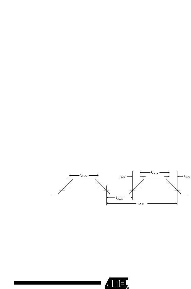
23.2External Clock Drive Waveforms
Figure 23-1. External Clock Drive Waveforms
VIH1
VIL1
0np
167
2586A–AVR–02/05
23.3External Clock Drive
Table 23-1. |
External Clock Drive |
|
|
|
|
|
|
|
|
|
|
|
VCC = 1.8 - 5.5V |
VCC = 2.7 - 5.5V |
VCC = 4.5 - 5.5V |
|
|||
Symbol |
|
Parameter |
Min. |
Max. |
Min. |
Max. |
Min. |
Max. |
Units |
|
|
|
|
|
|
|
|
|
|
1/tCLCL |
|
Clock Frequency |
0 |
4 |
0 |
10 |
0 |
20 |
MHz |
tCLCL |
|
Clock Period |
250 |
|
100 |
|
50 |
|
ns |
tCHCX |
|
High Time |
100 |
|
40 |
|
20 |
|
ns |
tCLCX |
|
Low Time |
100 |
|
40 |
|
20 |
|
ns |
tCLCH |
|
Rise Time |
|
2.0 |
|
1.6 |
|
0.5 |
µs |
tCHCL |
|
Fall Time |
|
2.0 |
|
1.6 |
|
0.5 |
µs |
∆tCLCL |
|
Change in period from one clock cycle to the next |
|
2 |
|
2 |
|
2 |
% |
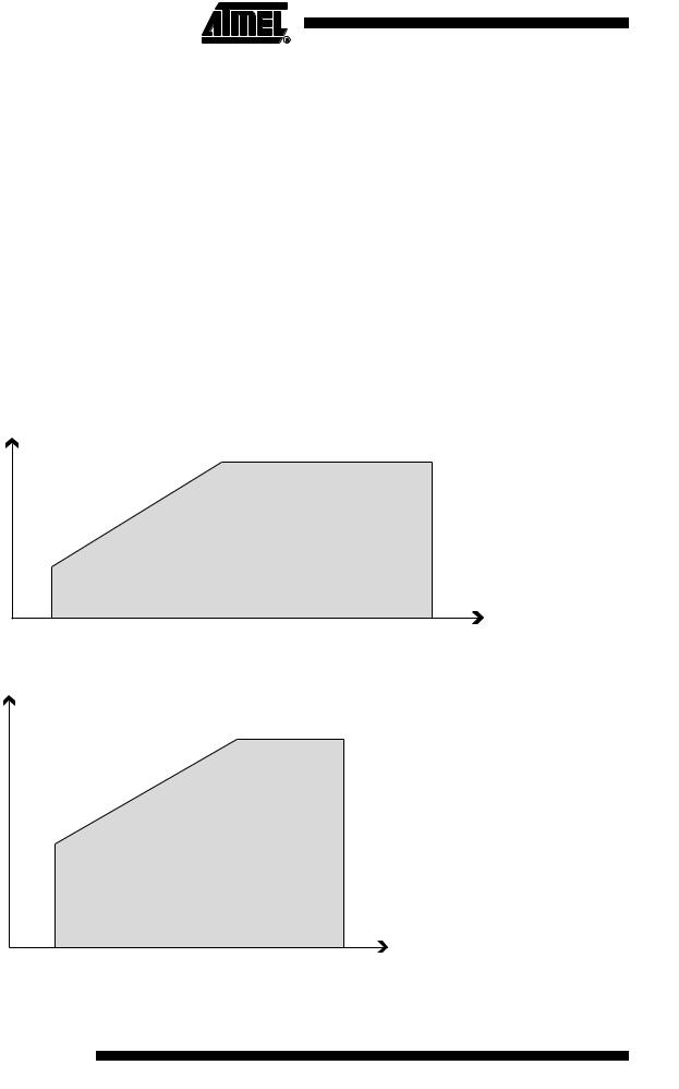
23.4Maximum Speed vs. VCC
Figure 23-2. |
Maximum Frequency vs. VCC |
|
|
|
10 MHz |
|
|
|
|
Safe Operating Area |
|
|
4 MHz |
|
|
|
1.8V |
2.7V |
5.5V |
Figure 23-3. |
Maximum Frequency vs. VCC |
|
|
|
20 MHz |
|
|
10 MHz
Safe Operating Area
2.7V |
4.5V |
5.5V |
168 ATtiny25/45/85
2586A–AVR–02/05

ATtiny25/45/85
23.5ADC Characteristics – Preliminary Data
Table 23-2. ADC Characteristics, Single Ended Channels. -40°C - 85°C
Symbol |
Parameter |
Condition |
Min(1) |
Typ(1) |
Max(1) |
Units |
|
Resolution |
Single Ended Conversion |
|
|
10 |
Bits |
|
|
|
|
|
|
|
|
|
Single Ended Conversion |
|
|
|
|
|
|
VREF = 4V, VCC = 4V, |
|
2 |
|
LSB |
|
|
ADC clock = 200 kHz |
|
|
|
|
|
|
|
|
|
|
|
|
|
Single Ended Conversion |
|
|
|
|
|
|
VREF = 4V, VCC = 4V, |
|
3 |
|
LSB |
|
Absolute accuracy (Including |
ADC clock = 1 MHz |
|
|
|
|
|
|
|
|
|
|
|
|
Single Ended Conversion |
|
|
|
|
|
|
INL, DNL, quantization error, |
|
|
|
|
|
|
VREF = 4V, VCC = 4V, |
|
|
|
|
|
|
gain and offset error) |
|
1.5 |
|
LSB |
|
|
|
ADC clock = 200 kHz |
|
|
||
|
|
|
|
|
|
|
|
|
Noise Reduction Mode |
|
|
|
|
|
|
|
|
|
|
|
|
|
Single Ended Conversion |
|
|
|
|
|
|
VREF = 4V, VCC = 4V, |
|
2.5 |
|
LSB |
|
|
ADC clock = 1 MHz |
|
|
||
|
|
|
|
|
|
|
|
|
Noise Reduction Mode |
|
|
|
|
|
|
|
|
|
|
|
|
|
Single Ended Conversion |
|
|
|
|
|
Integral Non-linearity (INL) |
VREF = 4V, VCC = 4V, |
|
1 |
|
LSB |
|
|
ADC clock = 200 kHz |
|
|
|
|
|
|
|
|
|
|
|
|
|
Single Ended Conversion |
|
|
|
|
|
Differential Non-linearity (DNL) |
VREF = 4V, VCC = 4V, |
|
0.5 |
|
LSB |
|
|
ADC clock = 200 kHz |
|
|
|
|
|
|
|
|
|
|
|
|
|
Single Ended Conversion |
|
|
|
|
|
Gain Error |
VREF = 4V, VCC = 4V, |
|
2.5 |
|
LSB |
|
|
ADC clock = 200 kHz |
|
|
|
|
|
|
|
|
|
|
|
|
|
Single Ended Conversion |
|
|
|
|
|
Offset Error |
VREF = 4V, VCC = 4V, |
|
1.5 |
|
LSB |
|
|
ADC clock = 200 kHz |
|
|
|
|
|
|
|
|
|
|
|
|
Conversion Time |
Free Running Conversion |
13 |
|
260 |
µs |
|
|
|
|
|
|
|
|
Clock Frequency |
|
50 |
|
1000 |
kHz |
|
|
|
|
|
|
|
VIN |
Input Voltage |
|
GND |
|
VREF |
V |
|
Input Bandwidth |
|
|
38.5 |
|
kHz |
|
|
|
|
|
|
|
VINT |
Internal Voltage Reference |
|
1.0 |
1.1 |
1.2 |
V |
RAIN |
Analog Input Resistance |
|
|
100 |
|
MΩ |
Note: 1. |
Values are preliminary. |
|
|
|
|
|
2.Minimum for AVCC is 1.8V.
3.Maximum for AVCC is 5.5V.
169
2586A–AVR–02/05

24. ATtiny25/45/85 Typical Characteristics – Preliminary Data - TBD
The data contained in this section is largely based on simulations and characterization of similar devices in the same process and design methods. Thus, the data should be treated as indications of how the part will behave.
The following charts show typical behavior. These figures are not tested during manufacturing. All current consumption measurements are performed with all I/O pins configured as inputs and with internal pull-ups enabled. A sine wave generator with rail-to-rail output is used as clock source.
The power consumption in Power-down mode is independent of clock selection.
The current consumption is a function of several factors such as: operating voltage, operating frequency, loading of I/O pins, switching rate of I/O pins, code executed and ambient temperature. The dominating factors are operating voltage and frequency.
The current drawn from capacitive loaded pins may be estimated (for one pin) as CL*VCC*f where
CL = load capacitance, VCC = operating voltage and f = average switching frequency of I/O pin.
The parts are characterized at frequencies higher than test limits. Parts are not guaranteed to function properly at frequencies higher than the ordering code indicates.
The difference between current consumption in Power-down mode with Watchdog Timer enabled and Power-down mode with Watchdog Timer disabled represents the differential current drawn by the Watchdog Timer.
170 ATtiny25/45/85 
2586A–AVR–02/05