


ATtiny25/45/85
14.1.9PLL Control and Status Register - PLLCSR
Bit |
7 |
6 |
5 |
4 |
3 |
2 |
1 |
0 |
|
$27 ($27) |
LSM |
- |
- |
- |
- |
PCKE |
PLLE |
PLOCK |
PLLCSR |
|
|
|
|
|
|
|
|
|
|
Read/Write |
R |
R |
R |
R |
R |
R/W |
R/W |
R |
|
Initial value |
0 |
0 |
0 |
0 |
0 |
0 |
0/1 |
0 |
|
• Bit 7- LSM: Low Speed Mode
The high speed mode is enabled as default and the fast peripheral clock is 64 MHz, but the low speed mode can be set by writing the LSM bit to one. Then the fast peripheral clock is scaled down to 32 MHz. The low speed mode must be set, if the supply voltage is below 2.7 volts, because the Timer/Counter1 is not running fast enough on low voltage levels. It is highly recommended that Timer/Counter1 is stopped whenever the LSM bit is changed.
• Bit 6.. 3- Res : Reserved Bits
These bits are reserved bits in the ATtiny25/45/85 and always read as zero.
• Bit 2- PCKE: PCK Enable
The PCKE bit change the Timer/Counter1 clock source. When it is set, the asynchronous clock mode is enabled and fast 64 MHz (or 32 MHz in Low Speed Mode) PCK clock is used as Timer/Counter1 clock source. If this bit is cleared, the synchronous clock mode is enabled, and system clock CK is used as Timer/Counter1 clock source. This bit can be set only if PLLE bit is set. It is safe to set this bit only when the PLL is locked i.e the PLOCK bit is 1. The bit PCKE can only be set, if the PLL has been enabled earlier.
• Bit 1- PLLE: PLL Enable
When the PLLE is set, the PLL is started and if needed internal RC-oscillator is started as a PLL reference clock. If PLL is selected as a system clock source the value for this bit is always 1.
• Bit 0- PLOCK: PLL Lock Detector
When the PLOCK bit is set, the PLL is locked to the reference clock, and it is safe to enable PCK for Timer/Counter1. After the PLL is enabled, it takes about 100 micro seconds for the PLL to lock.
14.1.10Timer/Counter1 Initialization for Asynchronous Mode
To change Timer/Counter1 to the asynchronous mode, first enable PLL, and poll the PLOCK bit until it is set, and then set the PCKE bit.
14.1.11Timer/Counter1 in PWM Mode
When the PWM mode is selected, Timer/Counter1 and the Output Compare Register C - OCR1C form a dual 8-bit, free-running and glitch-free PWM generator with outputs on the PB1(OC1A) and PB3(OC1B) pins and inverted outputs on pins PB0(OC1A) and PB2(OC1B). As default non-overlapping times for complementary output pairs are zero, but they can be inserted using a Dead Time Generator (see description on page 100).
93
2586A–AVR–02/05
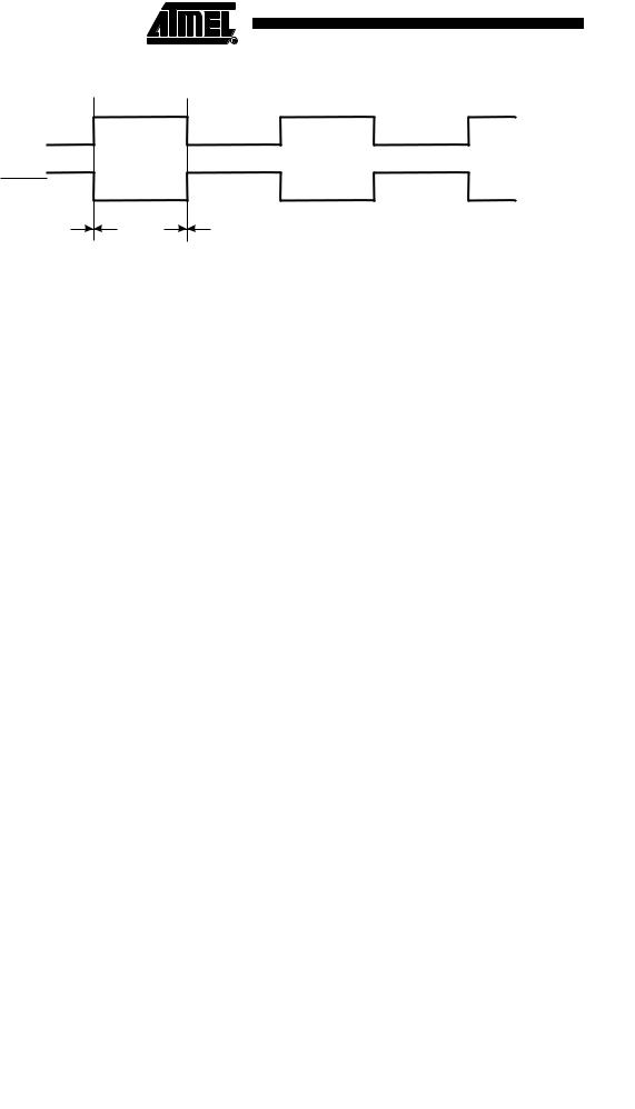
Figure 14-4. The PWM Output Pair
PWM1x
PWM1x
t non-overlap=0 t non-overlap=0 |
x = A or B |
When the counter value match the contents of OCR1A or OCR1B, the OC1A and OC1B outputs are set or cleared according to the COM1A1/COM1A0 or COM1B1/COM1B0 bits in the Timer/Counter1 Control Register A - TCCR1, as shown in Table 14-4.
Timer/Counter1 acts as an up-counter, counting from $00 up to the value specified in the output compare register OCR1C, and starting from $00 up again. A compare match with OC1C will set an overflow interrupt flag (TOV1) after a synchronization delay following the compare event.
Table 14-4. |
Compare Mode Select in PWM Mode |
||||
COM11 |
COM10 |
|
Effect on Output Compare Pins |
||
|
|
|
|
||
0 |
0 |
|
OC1x not connected. |
||
|
|
|
|||
OC1x not connected. |
|||||
|
|
|
|||
|
|
|
|
||
0 |
1 |
|
OC1x cleared on compare match. Set whenTCNT1 = $01. |
||
|
|
|
|||
OC1x set on compare match. Cleared when TCNT1 = $00. |
|||||
|
|
|
|||
|
|
|
|
||
1 |
0 |
|
OC1x cleared on compare match. Set when TCNT1 = $01. |
||
|
|
|
|||
OC1x not connected. |
|||||
|
|
|
|||
|
|
|
|
||
1 |
1 |
|
OC1x Set on compare match. Cleared when TCNT1= $01. |
||
|
|
|
|||
OC1x not connected. |
|||||
|
|
|
|||
|
|
|
|
|
|
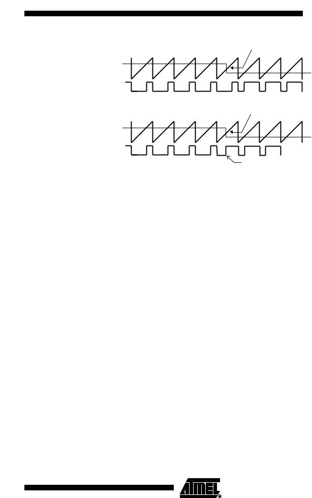
Note that in PWM mode, writing to the Output Compare Registers OCR1A or OCR1B, the data value is first transferred to a temporary location. The value is latched into OCR1A or OCR1B when the Timer/Counter reaches OCR1C. This prevents the occurrence of odd-length PWM pulses (glitches) in the event of an unsynchronized OCR1A or OCR1B. See Figure 14-5 for an example.
94 ATtiny25/45/85 
2586A–AVR–02/05
ATtiny25/45/85
Figure 14-5. Effects of Unsynchronized OCR Latching
Compare Value changes
Counter Value
Compare Value
PWM Output OC1x
Synchronized OC1x Latch
Compare Value changes
Counter Value
Compare Value
|
PWM Output OC1x |
Unsynchronized OC1x Latch |
Glitch |
During the time between the write and the latch operation, a read from OCR1A or OCR1B will read the contents of the temporary location. This means that the most recently written value always will read out of OCR1A or OCR1B.
When OCR1A or OCR1B contain $00 or the top value, as specified in OCR1C register, the output PB1(OC1A) or PB3(OC1B) is held low or high according to the settings of COM1A1/COM1A0. This is shown in Table 14-5.
Table 14-5. PWM Outputs OCR1x = $00 or OCR1C, x = A or B
|
|
|
|
|
|
|
COM1x1 |
COM1x0 |
OCR1x |
Output OC1x |
Output OC1x |
||
|
|
|
|
|
|
|
0 |
1 |
$00 |
L |
H |
||
|
|
|
|
|
|
|
0 |
1 |
OCR1C |
H |
L |
||
|
|
|
|
|
|
|
1 |
0 |
$00 |
L |
Not connected. |
||
|
|
|
|
|
|
|
1 |
0 |
OCR1C |
H |
Not connected. |
||
|
|
|
|
|
|
|
1 |
1 |
$00 |
H |
Not connected. |
||
|
|
|
|
|
|
|
1 |
1 |
OCR1C |
L |
Not connected. |
||
|
|
|
|
|
|
|
In PWM mode, the Timer Overflow Flag - TOV1 is set when the TCNT1 counts to the OCR1C value and the TCNT1 is reset to $00. The Timer Overflow Interrupt1 is executed when TOV1 is set provided that Timer Overflow Interrupt and global interrupts are enabled. This also applies to the Timer Output Compare flags and interrupts.
The frequency of the PWM will be Timer Clock 1 Frequency divided by (OCR1C value + 1). See the following equation:
ffTCK1
=-----------------------------------
PWM (OCR1C + 1)
Resolution shows how many bit is required to express the value in the OCR1C register. It is calculated by following equation
ResolutionPWM = log2(OCR1C + 1).
95
2586A–AVR–02/05

Table 14-6. Timer/Counter1 Clock Prescale Select in the Asynchronous Mode
PWM Frequency |
Clock Selection |
CS13:CS10 |
OCR1C |
RESOLUTION |
|
|
|
|
|
20 kHz |
PCK/16 |
0101 |
199 |
7.6 |
|
|
|
|
|
30 kHz |
PCK/16 |
0101 |
132 |
7.1 |
|
|
|
|
|
40 kHz |
PCK/8 |
0100 |
199 |
7.6 |
|
|
|
|
|
50 kHz |
PCK/8 |
0100 |
159 |
7.3 |
|
|
|
|
|
60 kHz |
PCK/8 |
0100 |
132 |
7.1 |
|
|
|
|
|
70 kHz |
PCK/4 |
0011 |
228 |
7.8 |
|
|
|
|
|
80 kHz |
PCK/4 |
0011 |
199 |
7.6 |
|
|
|
|
|
90 kHz |
PCK/4 |
0011 |
177 |
7.5 |
|
|
|
|
|
100 kHz |
PCK/4 |
0011 |
159 |
7.3 |
|
|
|
|
|
110 kHz |
PCK/4 |
0011 |
144 |
7.2 |
|
|
|
|
|
120 kHz |
PCK/4 |
0011 |
132 |
7.1 |
|
|
|
|
|
130 kHz |
PCK/2 |
0010 |
245 |
7.9 |
|
|
|
|
|
140 kHz |
PCK/2 |
0010 |
228 |
7.8 |
|
|
|
|
|
150 kHz |
PCK/2 |
0010 |
212 |
7.7 |
|
|
|
|
|
160 kHz |
PCK/2 |
0010 |
199 |
7.6 |
|
|
|
|
|
170 kHz |
PCK/2 |
0010 |
187 |
7.6 |
|
|
|
|
|
180 kHz |
PCK/2 |
0010 |
177 |
7.5 |
|
|
|
|
|
190 kHz |
PCK/2 |
0010 |
167 |
7.4 |
|
|
|
|
|
200 kHz |
PCK/2 |
0010 |
159 |
7.3 |
|
|
|
|
|
250 kHz |
PCK |
0001 |
255 |
8.0 |
|
|
|
|
|
300 kHz |
PCK |
0001 |
212 |
7.7 |
|
|
|
|
|
350 kHz |
PCK |
0001 |
182 |
7.5 |
|
|
|
|
|
400 kHz |
PCK |
0001 |
159 |
7.3 |
|
|
|
|
|
450 kHz |
PCK |
0001 |
141 |
7.1 |
|
|
|
|
|
500 kHz |
PCK |
0001 |
127 |
7.0 |
|
|
|
|
|
96 ATtiny25/45/85 
2586A–AVR–02/05