


UG-VIPSUITE |
Interrupts |
4-9 |
|
2015.01.23 |
|||
|
|
•For Clocked Video Output IP Core, the following steps reconfigure mode 1:
1.Write 0 to the Mode1 Valid register.
2.Write to the Mode 1 configuration registers.
3.Write 1 to the Mode1 Valid register. The mode is now valid and can be selected.
•For Clocked Video Output II IP Core, the following steps reconfigure mode 1:
1.Write 1 to the Bank Select register.
2.Write 0 to the Mode N Valid configuration register.
3.Write to the Mode N configuration registers, the Clocked Video Input II IP Core mirrors these writes internally to the selected bank.
4.Write 1 to the Mode N Valid register. The mode is now valid and can be selected.
You can configure a currently-selected mode in this way without affecting the video output of the CVO IP cores.
If there are multiple modes that match the resolution, the function selects the lowest mode. For example, the function selects Mode1 over Mode2 if both modes match. To allow the function to select Mode2, invalidate Mode1 by writing a 0 to its mode valid register. Invalidating a mode does not clear its configu ration.
Interrupts
The CVO IP cores produce a single interrupt line.
This interrupt line is the OR of the following internal interrupts:
•Status update interrupt—Triggers when the Video Mode Match register is updated by a new video mode being selected.
•Locked interrupt—Triggers when the outgoing video SOF is aligned to the incoming SOF.
Both interrupts can be independently enabled using bits [2:1] of the Control register. Their values can be read using bits [2:1] of the Interrupt register. Writing 1 to either of these bits clears the respective interrupt.
Generator Lock
Generator lock (Genlock) is the technique for locking the timing of video outputs to a reference source. Sources that are locked to the same reference can be switched between cleanly, on a frame boundary.
You can configure the IP cores to output, using vcoclk_div for CVO IP cores and refclk_div for CVI IP cores. With the exception of Clocked Video Input II IP core, these signals are divided down versions of vid_clk (vcoclk) and vid_clk (refclk) aligned to the start of frame (SOF). By setting the divided down value to be the length in samples of a video line, you can configure these signals to produce a horizontal reference.
For CVI IP cores, the phase-locked loop (PLL) can align its output clock to this horizontal reference. By tracking changes in refclk_div, the PLL can then ensure that its output clock is locked to the incoming video clock.
Note: For Clocked Video Input II IP core, the refclk_div signal is a pulse on the rising edge of the H sync which a PLL can align its output clock to.
Clocked Video Interface IP Cores |
Altera Corporation |
|
|
Send Feedback

4-10 |
Generator Lock |
UG-VIPSUITE |
|
2015.01.23 |
|||
|
|
A CVI IP core can take in the locked PLL clock and the SOF signal and align the output video to these signals. This produces an output video frame that is synchronized to the incoming video frame.
Clocked Video Input IP Core
For Clocked Video Input IP core, you can compare vcoclk_div to refclk_div, using a phase frequency detector (PFD) that controls a voltage controlled oscillator (VCXO). By controlling the VCXO, the PFD can align its output clock (vcoclk) to the reference clock (refclk). By tracking changes in the refclk_div signal, the PFD can then ensure that the output clock is locked to the incoming video clock.
You can set the SOF signal to any position within the incoming video frame. The registers used to configure the SOF signal are measured from the rising edge of the F0 vertical sync. Due to registering inside the settings of the CVI IP cores, the SOF Sample and SOF Line registers to 0 results in a SOF signal rising edge:
•six cycles after the rising edge of the V sync in embedded synchronization mode
•three cycles after the rising edge of the V sync in separate synchronization mode
A rising edge on the SOF signal (0 to 1) indicates the start of frame.
Table 4-6: Example of Clocked Video Input To Output an SOF Signal
The table below list an example of how to set up the Clocked Video Input IP core to output an SOF signal aligned to the incoming video synchronization (in embedded synchronization mode).
Format |
|
SOF Sample Register |
|
SOF Line Register |
|
Refclk Divider Register |
|
|
|
|
|
|
|
720p60 |
|
1644 << 2 |
|
749 |
|
1649 |
|
|
|
|
|
|
|
1080i60 |
|
2194 << 2 |
|
1124 |
|
2199 |
NTSC |
|
856 << 2 |
|
524 |
|
857 |
|
|
|
|
|
|
|
Altera Corporation |
Clocked Video Interface IP Cores |
|
|
Send Feedback
UG-VIPSUITE |
Underflow and Overflow |
4-11 |
|
2015.01.23 |
|||
|
|
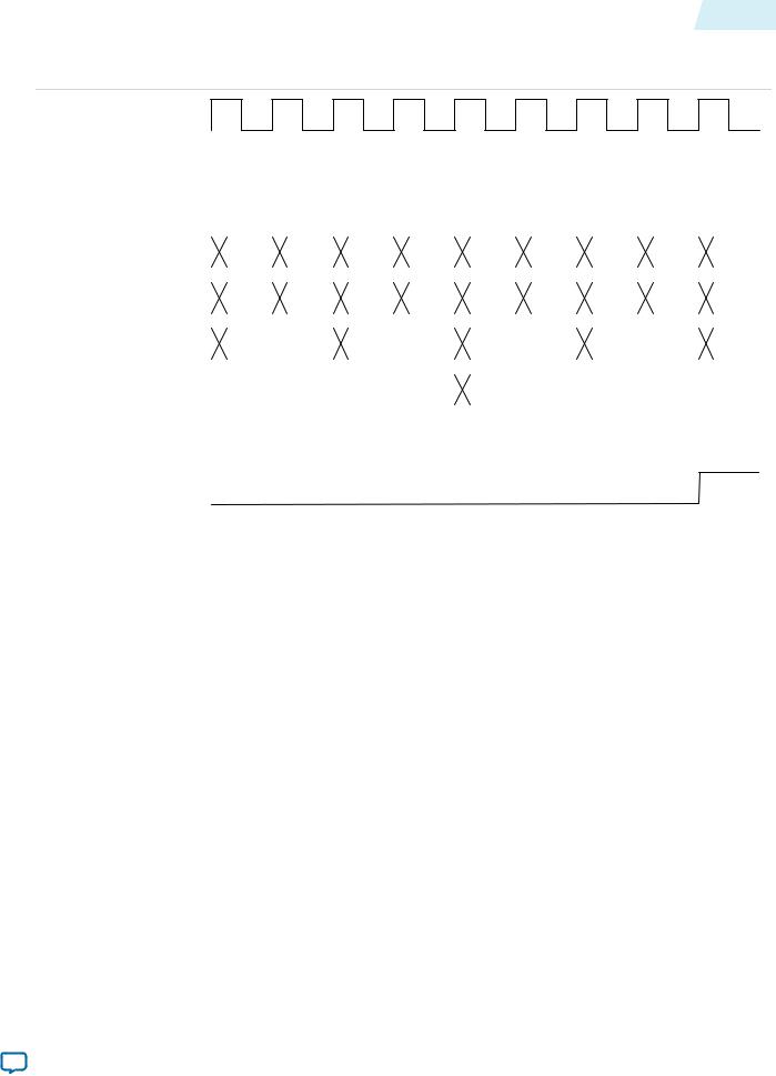
Figure 4-3: Genlock Example Configuration
The figure shows an example of a Genlock configuration for Clocked Video Input IP core.
F |
|
|
|
|
|
|
|
|
|
|
|
|
|
|
|
|
|
|
|
|
|
|
V Sync |
|
|
|
|
|
|
|
|
|
|
|
|
|
|
|
|
|
|
|
|
|
|
|
|
|
|
|
|
|
|
|
|
|
|
|
|
|
|
|
|
|
|
|
|
|
|
|
|
|
|
|
|
|
|
|
|
|
|
|
|
|
|
|
|
|
|
|
|
|
|
|
|
|
|
|
|
|
|
|
|
|
|
|
|
|
|
|
|
|
|
|
|
|
|
|
|
|
|
|
|
|
|
|
|
|
|
|
|
|
|
|
|
|
|
Data |
|
Cb |
|
|
Y |
|
|
Cr |
|
|
Y |
|
Cb |
|
Y |
|
Cr |
|
Y |
|
Cb |
|
|
|
|
|
|
|
|
|
|
|
|
|
|
|
|
|
|
|
|
|
|
|
|
|
|
|
|
|
|
|
|
|
|
|
|
|
|
|
|
|
|
|
|
|
|
|
SubSample |
0 |
1 |
0 |
1 |
0 |
1 |
0 |
1 |
0 |
|
||||||||||||
|
|
|
|
|
|
|
|
|
|
|
|
|
|
|
|
|
|
|
|
|
|
|
|
|
|
|
|
|
|
|
|
|
|
|
|
|
|
|
|
|
|
|
|
||
Sample |
|
|
856 |
|
|
|
|
857 |
|
|
|
0 |
|
|
|
1 |
|
2 |
|
|||
|
|
|
|
|
|
|
|
|
|
|
|
|
|
|
|
|
|
|
|
|
||
|
|
|
|
|
|
|
|
|
|
|
|
|
|
|
|
|
|
|
|
|
|
|
Line |
|
|
|
|
|
524 |
|
|
|
|
|
|
|
|
0 |
|
|
|
|
|
||
SOF |
|
|
|
|
|
|
|
|
|
|
|
|
|
|
|
|
|
|
|
|
|
|
|
|
|
|
|
|
|
|
|
|
|
|
|
|
|
|
|
|
|
|
|
|
|
(SOFSubSample = 0, |
|
|
|
|
|
|
|
|
|
|
|
|
|
|
|
|
|
|
|
|
|
|
SOFSample = 0, SOFLine = 0) |
|
|
|
|
|
|
|
|
|
|
|
|
|
|
|
|
|
|
|
|
|
|
|
|
|
|
|
|
|
|
|
|
|
|
|
|
|
|
|
|
|
|
|
|
|
SOF |
|
|
|
|
|
|
|
|
|
|
|
|
|
|
|
|
|
|
|
|
|
|
(SOFSubSample = 1, |
|
|
|
|
|
|
|
|
|
|
|
|
|
|
|
|
|
|
|
|
|
|
SOFSample = 1, SOFLine = 1) |
|
|
|
|
|
|
|
|
|
|
|
|
|
|
|
|
|
|
|
|
|
|
|
|
|
|
|
|
|
|
|
|
|
|
|
|
|
|
|
|
|
|
|
|
|
Clocked Video Input II IP Core
For Clocked Video Input II IP core, the SOF signal produces a pulse on the rising edge of the V sync. For interlaced video, the pulse is only produced on the rising edge of the F0 field, not the F1 field. A start of frame is indicated by a rising edge on the SOF signal (0 to 1).
Underflow and Overflow
Moving between the domain of clocked video and the flow controlled world of Avalon-ST Video can cause flow problems. The Clocked Video Interface IP cores contain a FIFO can accommodate any bursts in the flow data when set to a large enough value. The FIFO can accommodate any bursts as long as the input/output rate of the upstream/downstream Avalon-ST Video components is equal to or higher than that of the incoming/outgoing clocked video.
Underflow
The FIFO can accommodate any bursts as long as the output rate of the downstream Avalon-ST Video components is equal to or higher than that of the outgoing clocked video. If this is not the case, the FIFO underflows. If underflow occurs, the CVO IP cores continue to produce video and resynchronizing the startofpacket for the next image packet, from the Avalon-ST Video interface with the start of the next frame. You can detect the underflow by looking at bit 2 of the Status register. This bit is sticky and if an underflow occurs, it stays at 1 until the bit is cleared by writing a 1 to it.
Clocked Video Interface IP Cores |
Altera Corporation |
|
|
Send Feedback
4-12 |
Timing Constraints |
UG-VIPSUITE |
|
2015.01.23 |
|||
|
|
Note: For Clocked Video Output IP core, you can also read the current level of the FIFO from the Used Words register. This register is not available for Clocked Video Output II IP core.
Overflow
The FIFO can accommodate any bursts as long as the input rate of the upstream Avalon-ST Video components is equal to or higher than that of the incoming clocked video. If this is not the case, the FIFO overflows. If overflow occurs, the CVI IP cores produce an early endofpacket signal to complete the current frame. It then waits for the next start of frame (or field) before resynchronizing to the incoming clocked video and beginning to produce data again. The overflow is recorded in bit [9] of the Status register. This bit is sticky, and if an overflow occurs, it stays at 1 until the bit is cleared by writing a 0 to it. In addition to the overflow bit, you can read the current level of the FIFO from the Used Words register.
The height and width parameters at the point the frame was completed early will be used in the control packet of the subsequent frame. If you are reading back the detected resolution, then these unusual resolution values can make the CVI IP cores seem to be operating incorrectly where in fact, the downstream system is failing to service the CVI IP cores at the necessary rate.
Timing Constraints
You need to constrain the Clocked Video Interface IP cores.
Clocked Video Input and Clocked Video Output IP Cores
To constrain these IP cores correctly, add the following files to your Quartus II project:
•<install_dir>\ip\altera\clocked_video_input\ alt_vip_cvi.sdc
•<install_dir>\ip\altera\clocked_video_output\alt_vip_cvo.sdc
When you apply the .sdc file, you may see some warning messages in a format as follows:
•Warning: At least one of the filters had some problems and could not be matched.
•Warning: * could not be matched with a keeper.
These warnings are expected, because in certain configurations the Quartus II software optimizes unused registers and they no longer remain in your design.
Clocked Video Input II and Clocked Video Output II IP Cores
For these IP cores, the .sdc files are automatically included by their respective .qip files. After adding the Qsys system to your design in Quartus, verify that the alt_vip_cvi_core.sdc or alt_vip_cvo_core.sdc has been included.
Altera recommends that you place a frame buffer in any CVI to CVO system. Because the CVO II IP core generates sync signals for a complete frame, even when video frames end early, it is possible for the CVO II IP core to continually generate backpressure to the CVI II IP core so that it keeps ending packets early.
Handling Ancillary Packets
The Clocked Video Interface IP cores use Active Format Description (AFD) Extractor and Inserter examples to handle ancillary packets.
Altera Corporation |
Clocked Video Interface IP Cores |
|
|
Send Feedback

UG-VIPSUITE |
Handling Ancillary Packets |
4-13 |
|
2015.01.23 |
|||
|
|
AFD Extractor (Clocked Video Input)
When the output of the CVI IP cores connects to the input of the AFD Extractor, the AFD Extractor removes any ancillary data packets from the stream and checks the DID and secondary DID (SDID) of the ancillary packets contained within each ancillary data packet. If the packet is an AFD packet (DID = 0x41, SDID = 0x5), the extractor places the contents of the ancillary packet into the AFD Extractor register map.
You can get the AFD Extractor from <install_dir>\ip\altera\clocked_video_input\afd_example.
Table 4-7: AFD Extractor Register Map
Address |
|
Register |
|
Description |
|
|
|
|
|
0 |
|
Control |
|
• When bit 0 is 0, the core discards all packets. |
|
|
|
|
• When bit 0 is 1, the core passes through all non-ancillary |
|
|
|
|
packets. |
|
|
|
|
|
1 |
|
— |
|
Reserved. |
2 |
|
Interrupt |
|
When bit 1 is 1, the core detects a change to the AFD data |
|
|
|
|
and the sets an interrupt. Writing a 1 to bit 1 clears the |
|
|
|
|
interrupt. |
|
|
|
|
|
3 |
|
AFD |
|
Bits 0-3 contain the active format description code. |
4 |
|
AR |
|
Bit 0 contains the aspect ratio code. |
|
|
|
|
|
5 |
|
Bar data flags |
|
• When AFD is 0000 or 0100, bits 0-3 describe the contents |
|
|
|
|
of bar data value 1 and bar data value 2. |
|
|
|
|
• When AFD is 0011, bar data value 1 is the pixel number |
|
|
|
|
end of the left bar and bar data value 2 is the pixel number |
|
|
|
|
start of the right bar. |
|
|
|
|
• When AFD is 1100, bar data value 1 is the line number |
|
|
|
|
end of top bar and bar data value 2 is the line number |
|
|
|
|
start of bottom bar. |
|
|
|
|
|
6 |
|
Bar data value 1 |
|
Bits 0-15 contain bar data value 1 |
|
|
|
|
|
7 |
|
Bar data value 2 |
|
Bits 0-15 contain bar data value 2 |
8 |
|
AFD valid |
|
• When bit 0 is 0, an AFD packet is not present for each |
|
|
|
|
image packet. |
|
|
|
|
• When bit 0 is 1, an AFD packet is present for each image |
|
|
|
|
packet. |
|
|
|
|
|
Ancillary Packets (Clocked Video Input II)
When you turn on the Extract Ancillary Packets parameter in embedded sync mode, the CVO IP core extracts any ancillary packets that are present in the Y channel of the incoming video's vertical blanking. The ancillary packets are stripped of their TRS code and placed in a RAM. You can access these packets by reading from the Ancillary Packet register. The packets are packed end to end from their Data ID to their final user word.
The RAM is 16 bits wide—two 8-bit ancillary data words are packed at each address location. The first word is at bits 0–7 and the second word is at bits 8–15. A word of all 1's indicates that no further ancillary packets are present and can appear in either the first word position or the second word position.
Clocked Video Interface IP Cores |
Altera Corporation |
|
|
Send Feedback
4-14 |
Handling Ancillary Packets |
UG-VIPSUITE |
|
2015.01.23 |
|||
|
|
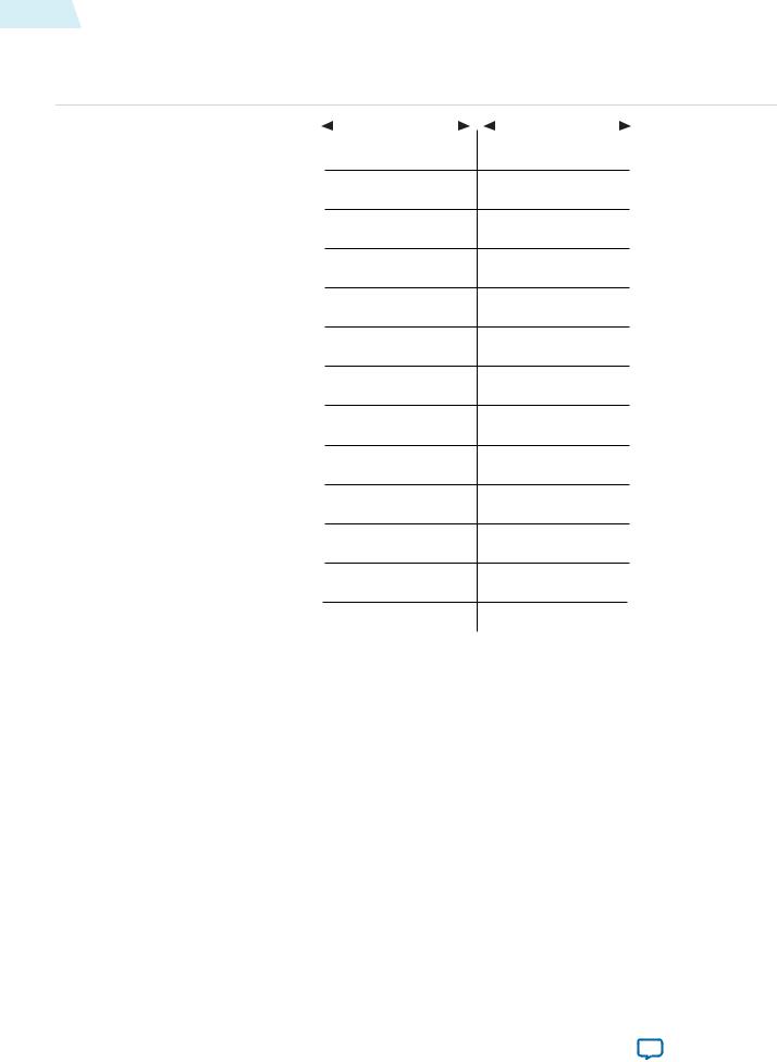
Figure 4-4: Ancillary Packet Register
The figure below shows the position of the ancillary packets. The different colors indicate different ancillary packets.
|
|
|
Bits 15–8 |
|
|
|
|
|
Bits 7–0 |
|
|
|
|
|
|
|
|
|
|
|
|
||||
Ancillary Address |
|
2nd Data ID |
|
|
|
Data ID |
|
|
||||
Ancillary Address +1 |
|
User Word 1 |
|
|
Data Count = 4 |
|
|
|||||
Ancillary Address +2 |
|
User Word 3 |
|
|
User Word 2 |
|
|
|||||
Ancillary Address +3 |
|
|
Data ID |
|
|
User Word 4 |
|
|
||||
Ancillary Address +4 |
|
Data Count = 5 |
|
|
2nd Data ID |
|
|
|||||
Ancillary Address +5 |
|
User Word 2 |
|
|
User Word 1 |
|
|
|||||
Ancillary Address +6 |
|
User Word 4 |
|
|
User Word 3 |
|
|
|||||
Ancillary Address +7 |
|
|
Data ID |
|
|
User Word 5 |
|
|
||||
Ancillary Address +8 |
|
Data Count = 7 |
|
|
2nd Data ID |
|
|
|||||
Ancillary Address +9 |
|
User Word 2 |
|
|
User Word 1 |
|
|
|||||
Ancillary Address +10 |
|
User Word 4 |
|
|
User Word 3 |
|
|
|||||
Ancillary Address +11 |
|
User Word 6 |
|
|
User Word 5 |
|
|
|||||
Ancillary Address +12 |
|
|
0×FF |
|
|
User Word 7 |
|
|
||||
|
|
|
|
|
|
|
|
|
|
|
|
|
|
|
|
|
|
|
|
|
|
|
|
|
|
Use the Depth of ancillary memory parameter to control the depth of the ancillary RAM. If available space is insufficient for all the ancillary packets, then excess packets will be lost. The ancillary RAM is filled from the lowest memory address to the highest during each vertical blanking period—the previous blanking periods packets are overwritten. To avoid missing ancillary packets, the ancillary RAM should be read every time the End of field/frame interrupt register triggers.
AFD Inserter (Clocked Video Output)
When the output of the AFD Inserter connects to the input of the CVO IP cores, the AFD Inserter inserts an Avalon-ST Video ancillary data packet into the stream after each control packet. The AFD Inserter sets the DID and SDID of the ancillary packet to make it an AFD packet (DID = 0x41, SDID = 0x5). The contents of the ancillary packet are controlled by the AFD Inserter register map.
You can get the AFD Extractor from <install_dir>\ip\altera\clocked_video_output\afd_example.
Altera Corporation |
Clocked Video Interface IP Cores |
|
|
Send Feedback