- •CONTENTS
- •FIGURES
- •TABLES
- •1.1 Manual Contents
- •1.2 Notational Conventions and Terminology
- •1.3 Related Documents
- •1.4 Application Support Services
- •2.1 Typical Applications
- •2.2 Microcontroller Features
- •2.3 Functional Overview
- •2.3.1 Core
- •2.3.1.3 Register File
- •2.3.2 Memory Controller
- •2.4 Internal Timing
- •2.4.1 Clock and Power Management Logic
- •2.4.2 Internal Timing
- •2.4.2.1 Clock Failure Detection Logic
- •2.4.2.2 External Timing
- •2.4.2.3 Power Management Options
- •2.4.3 Internal Memory
- •2.4.4 Serial Debug Unit
- •2.4.5 Interrupt Service
- •2.5 Internal Peripherals
- •2.5.1 I/O Ports
- •2.5.2 Serial I/O (SIO) Port
- •2.5.3 Synchronous Serial I/O (SSIO) Port
- •2.5.4 Event Processor Array (EPA) and Timer/Counters
- •2.5.7 Stack Overflow Module
- •2.5.8 Watchdog Timer
- •2.6 Special Operating Modes
- •2.7 Chip Configuration Registers
- •3.1 Overview of the Instruction Set
- •3.1.1 BIT Operands
- •3.1.2 BYTE Operands
- •3.1.4 WORD Operands
- •3.1.5 INTEGER Operands
- •3.1.9 Converting Operands
- •3.1.10 Conditional Jumps
- •3.1.11 Floating-Point Operations
- •3.1.12 Extended Instructions
- •3.2 Addressing Modes
- •3.2.1 Direct Addressing
- •3.2.2 Immediate Addressing
- •3.2.3 Indirect Addressing
- •3.2.3.1 Extended Indirect Addressing
- •3.2.3.2 Indirect Addressing with Autoincrement
- •3.2.3.3 Extended Indirect Addressing with Autoincrement
- •3.2.3.4 Indirect Addressing with the Stack Pointer
- •3.2.4 Indexed Addressing
- •3.2.4.3 Extended Indexed Addressing
- •3.2.4.4 Zero-indexed Addressing
- •3.3 Considerations for Crossing Page Boundaries
- •3.4 Software Protection Features and Guidelines
- •4.1 Memory Map Overview
- •4.2 Memory Partitions
- •4.2.1 External Memory
- •4.2.2 Internal ROM
- •4.2.2.1 Program Memory in Page FFH
- •4.2.2.3 Reserved Memory Locations
- •4.2.2.4 Interrupt, PIH, and PTS Vectors
- •4.2.2.5 Chip Configuration Bytes
- •4.2.3 Internal RAM (Code RAM)
- •4.2.4.2 Peripheral SFRs
- •4.2.5 Register File
- •4.2.5.2 Stack Pointer (SP)
- •4.3 Windowing
- •4.3.1 Selecting a Window
- •4.3.2 Addressing a Location Through a Window
- •4.3.2.4 Unsupported Locations Windowing Example
- •4.3.2.5 Using the Linker Locator to Set Up a Window
- •4.3.3 Windowing and Addressing Modes
- •4.4 Controlling Read Access to the Internal ROM
- •4.5 Remapping Internal ROM
- •5.1 Functional Overview
- •5.2 Stack Operations
- •5.3 Stack Overflow Module Registers
- •5.4 Programming the Stack Overflow Module
- •5.4.1 Initializing the Stack Pointer
- •5.4.2 Enabling the Stack Overflow Module and Specifying Stack Boundaries
- •6.1 Overview of the Interrupt Control Circuitry
- •6.2 Interrupt Signals and Registers
- •6.3 Interrupt Sources, Priorities, and Vector Addresses
- •6.3.1 PIH Interrupt Sources, Priorities, and Vector Addresses
- •6.3.1.1 Using Software to Provide the Vector Address
- •6.3.1.2 Providing the Vector Address in Response to a CPU Request
- •6.3.2 Special Interrupts
- •6.3.2.1 Unimplemented Opcode
- •6.3.2.2 Software Trap
- •6.3.2.4 Stack Overflow
- •6.3.3 External Interrupt Signal
- •6.3.4 Shared Interrupt Requests
- •6.4 Interrupt Latency
- •6.4.1 Situations that Increase Interrupt Latency
- •6.4.2 Calculating Latency
- •6.4.2.2 PTS Interrupt Latency
- •6.5 Programming the Interrupts
- •6.5.1 Modifying Interrupt Priorities
- •6.5.2 Determining the Source of an Interrupt
- •6.6 Initializing the PTS Control Blocks
- •6.6.1 Specifying the PTS Count
- •6.6.2 Selecting the PTS Mode
- •6.6.3 Single Transfer Mode
- •6.6.4 Block Transfer Mode
- •6.6.5 Dummy Mode
- •7.1 I/O Ports Overview
- •7.2 Configuring the Port Pins
- •7.2.2 Configuring Ports 3 and 4 (Address/Data Bus)
- •7.2.3 Port Configuration Example
- •7.3.1 Address and Data Signals (Ports 3, 4, and EPORT)
- •7.3.1.1 EPORT Status During Reset, CCB Fetch, Idle, Powerdown, and Hold
- •7.3.5 External Interrupt Signal (Port 2)
- •7.3.6 PWM Signals (Port 11)
- •7.3.7 Serial I/O Port Signals (Ports 2 and 7)
- •7.3.8 Special Operating Mode Signal (Port 5 Pin 7)
- •7.3.9 Synchronous Serial I/O Port Signals (Port 10)
- •7.4 I/O Port Internal Structures
- •7.4.3 Internal Structure for Ports 3 and 4 (Address/Data Bus)
- •8.1 Serial I/O (SIO) Port Functional Overview
- •8.2 Serial I/O Port Signals and Registers
- •8.3 Serial Port Modes
- •8.3.1 Synchronous Mode (Mode 0)
- •8.3.2 Asynchronous Modes (Modes 1, 2, and 3)
- •8.3.2.1 Mode 1
- •8.3.2.2 Mode 2
- •8.3.2.3 Mode 3
- •8.3.2.4 Multiprocessor Communications
- •8.4 Programming the Serial Port
- •8.4.1 Configuring the Serial Port Pins
- •8.4.2 Programming the Control Register
- •8.4.3 Programming the Baud Rate and Clock Source
- •8.4.4 Enabling the Serial Port Interrupts
- •8.4.5 Determining Serial Port Status
- •CHAPTER 9 Synchronous Serial I/O (SSIO) Port
- •9.1 SSIO Port Overview
- •9.1.1 Standard Mode
- •9.1.2 Duplex Mode
- •9.2 SSIO pORT sIGNALS AND rEGISTERS
- •9.3 ssio Port Operation
- •9.3.1 Transmitting and Receiving Data
- •9.3.1.1 Normal Transfers (All Modes)
- •9.3.1.2 Handshaking Transfers (Standard Mode Only)
- •9.4 Programming the SSIO Port
- •9.4.1 Configuring the SSIO Port Pins
- •9.4.2 Configuring the SSIO Registers
- •9.4.2.1 The SSIO Baud (SSIO_BAUD) Register
- •9.4.2.3 The SSIO 0 Clock (SSIO0_CLK) Register
- •9.4.2.4 The SSIO 1 Clock (SSIO1_CLK) Register
- •9.4.3 Enabling the SSIO Interrupts
- •9.5 Programming Considerations
- •9.5.2 Standard Mode Considerations
- •9.5.3 Duplex Mode Considerations
- •10.1 PWM FUNCTIONAL OVERVIEW
- •10.2 PWM Signals and Registers
- •10.3 pwm operation
- •10.4 Programming the Frequency and Period
- •10.5 Programming the Duty Cycle
- •10.5.1 Sample Calculations
- •10.5.2 Reading the Current Value of the Down-counter
- •10.5.3 Enabling the PWM Outputs
- •10.5.4 Generating Analog Outputs
- •11.1 EPA Functional Overview
- •11.2 EPA and Timer/Counter Signals and Registers
- •11.3 Timer/Counter Functional Overview
- •11.3.1 Timer Multiplexing on the Time Bus
- •11.4 EPA Channel Functional Overview
- •11.4.1 Operating in Input Capture Mode
- •11.4.2 Operating in Output Compare Mode
- •11.4.3 Operating in Compare Mode with the Output/Simulcapture Channels
- •11.4.4 Generating a 32-bit Time Value
- •11.4.5 Controlling a Pair of Adjacent Pins
- •11.5 Programming the EPA and Timer/Counters
- •11.5.1 Configuring the EPA and Timer/Counter Signals
- •11.5.2 Programming the Timers
- •11.5.3 Programming the Capture/Compare Channels
- •11.5.4 Programming the Compare-only (Output/Simulcapture) Channels
- •11.6 Enabling the EPA Interrupts
- •11.7 Determining Event Status
- •CHAPTER 12 Analog-to-digital (A/D) Converter
- •12.1 A/D Converter Functional Overview
- •12.2 A/D Converter Signals and Registers
- •12.3 A/D Converter Operation
- •12.4 Programming the A/D Converter
- •12.4.1 Programming the A/D Test Register
- •12.4.2 Programming the A/D Result Register (for Threshold Detection Only)
- •12.4.3 Programming the A/D Time Register
- •12.4.4 Programming the A/D Command Register
- •12.4.5 Programming the A/D Scan Register
- •12.4.6 Enabling the A/D Interrupt
- •12.5 Determining A/D Status and Conversion Results
- •12.6 Design Considerations
- •12.6.1 Designing External Interface Circuitry
- •12.6.1.1 Minimizing the Effect of High Input Source Resistance
- •12.6.1.2 Suggested A/D Input Circuit
- •12.6.1.3 Analog Ground and Reference Voltages
- •12.6.2 Understanding A/D Conversion Errors
- •CHAPTER 13 Minimum Hardware Considerations
- •13.1 Minimum Connections
- •13.1.1 Unused Inputs
- •13.1.2 I/O Port Pin Connections
- •13.2 Applying and Removing Power
- •13.3 Noise Protection Tips
- •13.4 The On-chip Oscillator Circuitry
- •13.5 Using an External Clock Source
- •13.6 Resetting the Microcontroller
- •13.6.1 Generating an External Reset
- •13.6.2 Issuing the Reset (RST) Instruction
- •13.6.3 Issuing an Illegal IDLPD Key Operand
- •13.6.4 Enabling the Watchdog Timer
- •13.6.5 Detecting Clock Failure
- •13.7 Identifying the Reset Source
- •14.1 Special Operating Mode Signals and Registers
- •14.2 Reducing Power Consumption
- •14.3 Idle Mode
- •14.3.1 Enabling and Disabling Idle Mode
- •14.3.2 Entering and Exiting Idle Mode
- •14.4 Powerdown Mode
- •14.4.1 Enabling and Disabling Powerdown Mode
- •14.4.2 Entering Powerdown Mode
- •14.4.3 Exiting Powerdown Mode
- •14.4.3.1 Generating a Hardware Reset
- •14.4.3.2 Asserting the External Interrupt Signal
- •14.4.3.3 Selecting an External Capacitor
- •14.5 ONCE Mode
- •CHAPTER 15 Interfacing with External Memory
- •15.1 Internal and External Addresses
- •15.2 External Memory Interface Signals and Registers
- •15.3 The Chip-select Unit
- •15.3.1 Defining Chip-select Address Ranges
- •15.3.2 Controlling Bus Parameters
- •15.3.3 Chip-select Unit Initial Conditions
- •15.3.4 Programming the Chip-select Registers
- •15.3.5 Example of a Chip-select Setup
- •15.4 Chip Configuration Registers and Chip Configuration Bytes
- •15.5 Bus Width and Multiplexing
- •15.5.1 A 16-bit Example System
- •15.5.2 16-bit Bus Timings
- •15.5.3 8-bit Bus Timings
- •15.5.4 Comparison of Multiplexed and Demultiplexed Buses
- •15.6 Wait States (Ready Control)
- •15.7 Bus-hold Protocol
- •15.7.1 Enabling the Bus-hold Protocol
- •15.7.2 Disabling the Bus-hold Protocol
- •15.7.3 Hold Latency
- •15.7.4 Regaining Bus Control
- •15.8 Write-control Modes
- •15.9 System Bus AC Timing Specifications
- •15.9.1 Deferred Bus-cycle Mode
- •15.9.2 Explanation of AC Symbols
- •15.9.3 AC Timing Definitions
- •16.1 Serial Debug Unit (SDU) Functional Overview
- •16.2 SDU Signals and Registers
- •16.3 SDU Operation
- •16.3.1 SDU State Machine
- •16.3.2 Code RAM Access State Machine
- •16.3.3 Minimizing Latency
- •16.4 Code RAM Access
- •16.4.1 Code RAM Data Transfer
- •16.4.2 Code RAM Access Instructions
- •16.4.3 Code RAM Data Transfer Example
- •16.5 SDU Interface Connector
- •17.1 Signals and Registers
- •17.2 Memory Protection Options
- •17.3 Entering Test-ROM Routines
- •17.3.1 Power-up and Power-down Sequences
- •17.4 ROM-dump Routine and Circuit
- •17.5 Serial Port Mode Routine
- •17.5.1 Serial Port RISM
- •17.5.2 Serial Port Mode Circuit
- •17.6 SDU RISM Execution Routine
- •17.6.1 SDU RISM Data Transfer
- •17.6.1.1 SDU RISM Data Transfer Before
- •17.6.1.2 SDU RISM Data Transfer After
- •17.6.2 SDU RISM Execution Circuit
- •17.7 RISM Command Descriptions
- •17.8 Executing Programs from Register RAM
- •17.9 RISM Command Examples
- •17.9.1 Serial Port Mode RISM Read Command Example
- •17.9.2 Serial Port Mode RISM Write Command Example
- •17.9.3 SDU RISM Execution Write Command Example
- •17.9.4 SDU RISM Execution Go Command Example
- •B.1 Functional Groupings of Signals
- •B.2 Signal Descriptions
- •B.3 Default Conditions
CHAPTER 5
STACK OVERFLOW MODULE
The stack overflow module monitors the value of the stack pointer (SP) and generates a nonmaskable interrupt request if the value is outside the boundaries you specify. This module helps to ensure data integrity. Without the stack overflow module, the stack could grow too large and corrupt other data, causing a fatal system error.
5.1FUNCTIONAL OVERVIEW
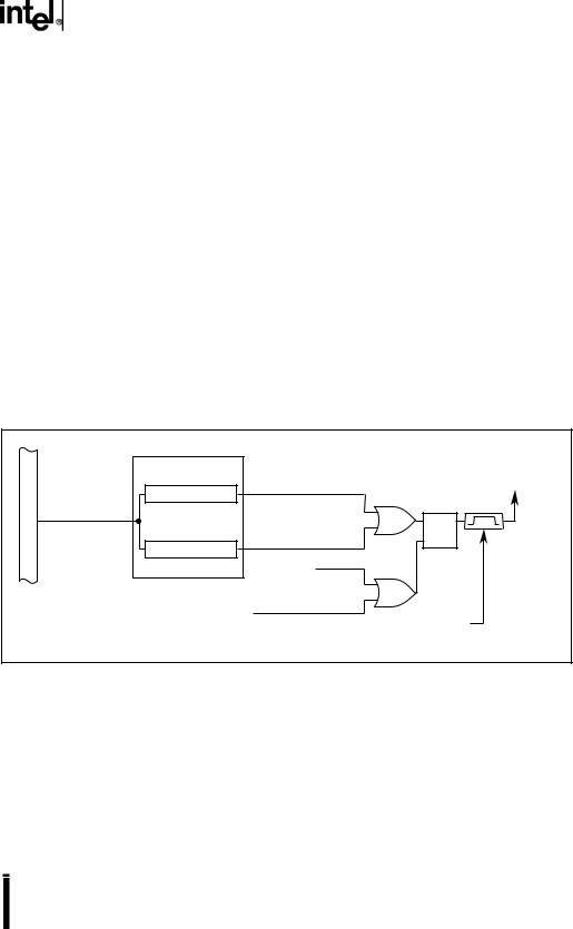
The stack overflow module (Figure 5-1) decodes the stack pointer addresses (0018–0019H) from the peripheral address bus. The comparator compares that value to the boundaries you specify. A stack pointer value that is equal to or outside the boundaries sets the R/S flip-flop, which in turn sets the nonmaskable interrupt pending bit.
The R/S flip-flop can be set only once, and only a reset or another write operation to the STACK_TOP register can clear it. Your initialization code and your interrupt service routine for the stack overflow error must write to the STACK_TOP register to enable the stack overflow module.
Bus |
Comparator |
|
|
|
SP ³ STACK_TOP |
|
Set INT_PEND1.6 |
||
Address |
|
|||
STACK_TOP |
|
|
||
Stack Pointer (SP) |
S |
Q |
||
|
||||
Peripheral |
0018–0019H |
|||
|
|
|||
SP £ STACK_BOTTOM |
R Q# |
|||
STACK_BOTTOM |
|
|
||
Reset |
|
|
||
|
|
|
||
|
Write to STACK_TOP |
|
|
|
|
|
One-shot |
||
|
|
pulse generator |
||
|
|
|
A3313-01 |
Figure 5-1. Stack Overflow Module Block Diagram
5.2STACK OPERATIONS
The stack is a last-in-first-out (LIFO) register used to keep track of program addresses and the processor status word (PSW), as well as to pass parameters from one routine to another. You control the location of the stack by initializing the stack pointer (SP) with an address that is two bytes (for 64-Kbyte mode) or four bytes (for 2-Mbyte mode) greater than the starting address (top) of the stack. The stack grows downward as entries are added (PUSHed onto the stack) and shrinks upward as entries are unloaded (POPped off the stack). The stack must be located in page 00H, and is most efficient when located in the upper register file.
5-1
8XC196EA USER’S MANUAL
When the CPU encounters a subroutine call or interrupt service routine, it manipulates the stack pointer (SP), the stack, and the program counter (PC) as shown in Table 5-1.
Table 5-1. Effect of Subroutine Execution on the Stack, SP, and PC
Instruction |
Operation |
BR, CALL, JUMP |
SP ← (SP–2) in 64-Kbyte mode or (SP–4) in 2-Mbyte mode) |
|
Stack ← PC (next instruction address) |
|
PC ← address of subroutine or interrupt service routine |
…Execute subroutine or interrupt service routine
RET |
PC ← next instruction address (from top of stack) |
|
SP ← (SP+2) in 64-Kbyte mode or (SP+4) in 2-Mbyte mode) |
5.3STACK OVERFLOW MODULE REGISTERS
Table 5-2 describes the registers associated with the stack overflow module.
Table 5-2. Stack Overflow Module Control and Status Registers
Mnemonic |
Address |
Description |
|
|
|
INT_MASK1 |
0013H |
Interrupt Mask 1 |
|
|
The stack overflow interrupt is always enabled. The nonfunctional |
|
|
STACK mask bit in INT_MASK1 exists for design symmetry with the |
|
|
INT_PEND1 register. Write zero to the STACK bit or leave it in its |
|
|
default state. |
|
|
|
INT_PEND1 |
0012H |
Interrupt Pending 1 |
|
|
The STACK bit in this register, when set, indicates that a stack |
|
|
overflow interrupt is pending. |
|
|
|
SP |
0018H |
Stack Pointer |
|
|
Initialize the stack pointer to an address that is two bytes (in 64-Kbyte |
|
|
mode) or four bytes (in 2-Mbyte mode) greater than the desired |
|
|
starting address (top) of the stack. Ensure that this value is within the |
|
|
boundaries you specify in STACK_BOTTOM and STACK_TOP. |
|
|
|
STACK_BOTTOM |
1FA0H |
Lower Stack Limit |
|
|
Write the boundary address for the bottom of the stack to this |
|
|
register. A stack pointer value that is equal to or less than this |
|
|
address will set the stack overflow interrupt pending bit in |
|
|
INT_PEND1. |
|
|
|
STACK_TOP |
1FA2H |
Upper Stack Limit |
|
|
You must write to this register to enable the stack overflow module |
|
|
after a reset and after a stack overflow. Write the boundary address |
|
|
for the top of the stack to this register. A stack pointer value that is |
|
|
equal to or greater than this address will set the stack overflow |
|
|
interrupt pending bit in INT_PEND1. |
|
|
|
5-2