


SERIAL I/O (SIO) PORT
Each channel has a receive interrupt (RIx) and a transmit interrupt (TIx) that indicate when the receive buffer is full or the transmit buffer is empty. Additionally, the serial port status (SPx_STATUS) register contains RI and TI flags. During a reception, the SIO sets the RI flag in SPx_STATUS after it samples the eighth data bit. The RIx pending bit in the interrupt pending register is set immediately before the RI flag is set. During a transmission, the SIO sets the TI flag immediately after it transmits the eighth data bit unless a delay is programmed. The SIO can delay the setting of the TI flag by one, three, or seven bit times. (See “Programming the Control Register” on page 8-11.) The TI x pending bit in the interrupt pending register is set when the TI flag in SPx_STATUS is set.
In mode 0, the receiver must be enabled for receptions and disabled for transmissions. (The SPx_CON register contains a bit that enables or disables the receiver. See “Programming the Control Register” on page 8-11.) When the receiver is enabled, clearing the receive interrupt (RI) flag in SPx_STATUS starts a reception. When the receiver is disabled, writing to SBUFx_TX starts a transmission.
Disabling the receiver stops a reception in progress and inhibits further receptions. When the receiver is enabled, clearing the RI flag in SPx_STATUS starts a reception; therefore, to avoid a corrupted reception, disable the receiver before clearing the RI flag. This can be handled in an interrupt environment by using software flags or in straight-line code by polling the interrupt pending register to signal the completion of a reception.
8.3.2Asynchronous Modes (Modes 1, 2, and 3)
Modes 1, 2, and 3 are full-duplex serial modes, meaning that they have dedicated receive and transmit data signals. Mode 1 is the standard eight-bit, asynchronous mode used for normal serial communications. With parity disabled, mode 1 transmits or receives eight data bits; with parity enabled, mode 1 transmits or receives seven data bits and a parity bit. Modes 2 and 3 are nine-bit asynchronous modes typically used for interprocessor communications (see “Multiprocessor Communications” on page 8-10). Like mode 1, mode 3 has optional parity. With parity disabled, mode 3 transmits or receives nine data bits; with parity enabled, mode 3 transmits or receives eight data bits and a parity bit.
When the serial port is configured for mode 1, 2, or 3, writing to SBUFx_TX causes the serial port to start transmitting data. (The transmitter transfers the data to the transmit shift register and starts shifting the data out through TXDx.) New data placed in SBUFx_TX is transferred to the shift register only after the stop bit of the previous data has been sent. If the receiver is enabled, a falling edge on the RXDx input causes the serial port to begin receiving data. Disabling the receiver stops a reception in progress and inhibits further receptions. (See “Programming the Control Register” on page 8-11.)
To minimize noise-related errors, the SIO samples the data line three times and uses majority logic to identify a valid start bit. That is, if two of the three samples are low, the bit is a valid start bit.
8-7

8XC196EA USER’S MANUAL
8.3.2.1Mode 1
Mode 1 is the standard asynchronous communications mode with optional parity. If parity is enabled, the receiver checks for even or odd parity, and the transmitter sends data with even or odd parity. When parity is disabled, the data frame used in this mode () consists of ten bits: a start bit (0), eight data bits (LSB first), and a stop bit (1). When parity is enabled, the eighth data bit becomes the parity bit; therefore, the data frame consists of a start bit (0), seven data bits (LSB first), a parity bit, and a stop bit (1).
Stop |
Start |
D0 |
D1 |
D2 |
D3 |
D4 |
D5 |
D6 |
D7 |
Stop |
8 Bits of Data or 7 Bits of Data with Parity Bit
10-bit Frame
A0245-02
Figure 8-4. Serial Port Frames for Mode 1
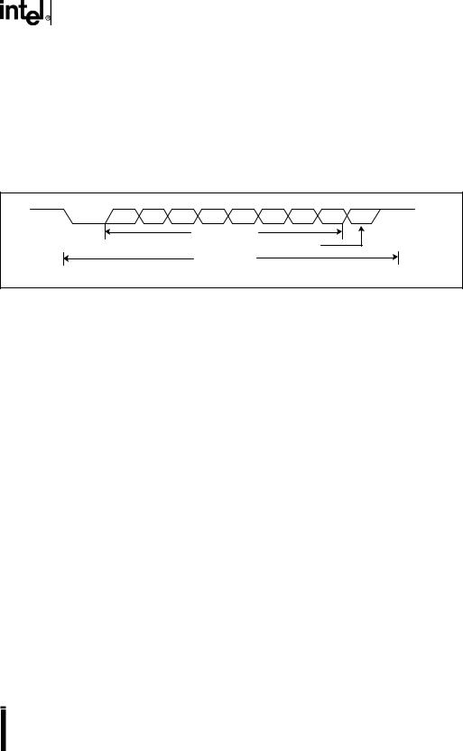
The transmit and receive functions are controlled by separate shift clocks. The baud-rate generator controls both the transmit and receive shift clocks. The transmit shift clock starts when the baud-rate generator is initialized. The receive shift clock is reset when a start bit (falling edge) is received. Therefore, the transmit clock may not be synchronized with the receive clock, although both will be at the same frequency.
The SIO sets the transmit interrupt (TI) and receive interrupt (RI) flags in SPx_STATUS to indicate completed operations. During a reception, the SIO sets both the RI flag and the RIx interrupt pending bit just before it receives the end of the stop bit. During a transmission, the SIO sets the TI flag immediately after it starts to transmit the stop bit unless a delay is programmed. The SIO can delay the setting of the TI flag by one, three, or seven bit times. (See “Programming the Control Register” on page 8-11.)
When connecting more than two microcontrollers with the serial port in half-duplex (that is, using a single data signal for both transmit and receive operations), it is important to wait for a reception to complete before starting to transmit. The receiving processor must wait for one bit time after the RI flag is set before starting to transmit. Otherwise, the transmission could corrupt the stop bit, causing a problem for other microcontrollers listening on the link. In addition to the receive interrupt pending bit (RIx), which indicates that the reception will be complete in one bit time, the serial port status (SPx_STATUS) register contains a reception in progress (RIP) bit. The SIO sets RIP at the start of a reception and clears it after the completion of a reception. (See “Determining Serial Port Status” on page 8-16.)
8-8
SERIAL I/O (SIO) PORT
8.3.2.2Mode 2
Mode 2 is the asynchronous, ninth-bit recognition mode. shows the data frame used in this mode. It consists of a start bit (0), nine data bits (LSB first), and a stop bit (1). During transmissions, write data bits 0–7 to the transmit buffer (SBUF x_TX) and write data bit 8 (the ninth data bit) to the transmit bit 8 (TB8) bit in the serial port control (SPx_CON) register. The SIO clears the TB8 bit after every transmission, so you must set it (if desired) before each write to SBUFx_TX. During receptions, the receive buffer (SBUFx_RX) contains data bits 0–7, and bit 7 in the serial port status (SPx_STATUS) register contains data bit 8 (the ninth data bit received).
Stop |
Start |
D0 |
D1 |
D2 |
D3 |
D4 |
D5 |
D6 |
D7 |
D8 |
Stop |
|
|
|
|
|
8 Bits of Data |
|
|
|
|
|
|
|
|
|
|
|
|
Programmable 9th Bit |
|
|
|
||
|
|
|
|
|
11-bit Frame |
|
|
|
|
|
|
|
|
|
|
|
|
|
|
|
|
|
A0111-01 |
Figure 8-5. Serial Port Frames in Mode 2 and 3
As in mode 1, in mode 2, the SIO sets the transmit interrupt (TI) flag in SPx_STATUS to indicate completed transmissions. During a transmission, the SIO sets the TI flag immediately after it starts to transmit the stop bit unless a delay is programmed. The SIO can delay the setting of the TI flag by one, three, or seven bit times. (See “Programming the Control Register” on page 8-11.) Unlike mode 1, in mode 2, the SIO sets the receive interrupt (RI) flag in SPx_STATUS only when the ninth data bit received is set. During a reception, when the ninth data bit is set, both the RI flag and the RIx interrupt pending bit are set just before the end of the stop bit. This feature provides an easy way to have selective reception on a data link. (See “Multiprocessor Communications” on page 8-10.) Parity is not available in mode 2.
8.3.2.3Mode 3
Mode 3 is the asynchronous, ninth-bit mode with optional parity. The data frame for this mode is identical to that of mode 2 (Figure 8-5 on page 8-9). Mode 3 differs from mode 2 during transmissions in that parity can be enabled, in which case the ninth bit becomes the parity bit. When parity is disabled, data bits 0–7 are written to the serial port transmit buffer (SBUF x_TX), and the ninth data bit is written to SPx_CON.4 (TB8). In mode 3, a reception always sets the RIx interrupt pending bit, regardless of the state of the ninth bit. If parity is disabled, the SPx_STATUS register bit 7 (RB8) contains the ninth data bit received. If parity is enabled, then the SPx_STATUS register bit 7 becomes the received parity error (RPE) flag.
8-9