

8XC196EA USER’S MANUAL
If the microcontroller is reset while in hold, bus contention can occur. For example, a device without internal ROM would try to fetch the chip configuration byte from external memory after RESET# was brought high. Bus contention would occur because both the external device and the microcontroller would attempt to access memory. One solution is to use the RESET# signal as the system reset; then all bus masters (including the microcontroller) are reset at once. Chapter 14, “Special Operating Modes,”shows system reset circuit examples.
15.8 WRITE-CONTROL MODES
The microcontroller has two write-control modes: the standard mode, which uses the WR# and BHE# signals; and the write strobe mode, which uses the WRL# and WRH# signals. Otherwise, the two modes are identical. The modes are selected by chip configuration register 0 (Figure 15-6 on page 15-17.)
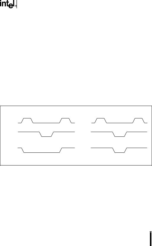
Figure 15-16 shows the waveforms of the asserted write-control signals in the two modes. Note that only BHE# is valid throughout the bus cycle.
Standard Mode |
Write Strobe Mode |
ALE |
ALE |
WR# |
WRL# |
Active for lowor high-byte write. |
Active for low-byte write. |
BHE# |
WRH# |
Active for high-byte write. |
Active for high-byte write. |
A2472-02
Figure 15-16. Write-control Signal Waveforms
compares the values of the write-control signals for write operations in the standard mode and the write strobe mode. The table lists values of WR# and BHE# and values of WRL# and WRH# for byte and word writes on a 16-bit and an 8-bit bus.
15-36

INTERFACING WITH EXTERNAL MEMORY
Table 15-10. Write Signals for Standard and Write Strobe Modes
Bus |
Word/Byte |
|
Standard |
Write Strobe |
|||
A0 or AD0† |
(CCR0.2 = 1) |
(CCR0.2 = 0) |
|||||
Width |
Written |
|
|
|
|
|
|
|
WR# |
|
BHE# |
WRL# |
WRH# |
||
|
|
|
|
||||
|
|
|
|
|
|
|
|
|
Low Byte |
0 |
0 |
|
1 |
0 |
1 |
|
|
|
|
|
|
|
|
16 |
High Byte |
1 |
0 |
|
0 |
1 |
0 |
|
|
|
|
|
|
|
|
Word |
0 |
0 |
|
0 |
0 |
0 |
|
|
|
||||||
|
|
|
|
|
|
|
|
|
1 |
|
Illegal |
Illegal |
|||
|
|
|
|||||
|
|
|
|
|
|
|
|
8 |
Low Byte |
0 |
0 |
|
1 |
0 |
1 |
|
|
|
|
|
|
|
|
High Byte |
1 |
0 |
|
1 |
0 |
1 |
|
|
|
||||||
|
|
|
|
|
|
|
|
† A0 for a demultiplexed address bus; AD0 for a multiplexed address/data bus.
To select the standard write-control mode, set CCR0.2. In standard mode, the WR#/WRL# pin operates as WR#, and the BHE#/WRH# pin operates as BHE#. WR# is asserted for every external memory write. BHE# is asserted for word accesses (read and write) and for byte accesses to odd addresses. BHE# can be used to select the bank of memory that stores the high (odd) byte. Figure 15-10 on page 15-25 illustrates use of the standard mode in a 16-bit system. In this example, WR# writes words to the 16-bit flash memory. To write individual bytes, you can use the decoding logic in Figure 15-17 or use the write strobe mode.
To write single bytes on a 16-bit bus requires separate low-byte and high-byte write signals (WRL# and WRH#). Figure 15-17 shows a sample circuit that combines WR#, BHE#, and address bit 0 (A0 for a demultiplexed address bus, AD0 for a mulitplexed address/data bus) to produce these signals. This additional logic is unnecessary, however. In the write strobe mode, WRL# and WRH# are available at the microcontroller’s external pins.
15-37

8XC196EA USER’S MANUAL
Demultiplexed Mode
BHE# 

WRH#
WR# 

WRL#
A0
Multiplexed Mode
BHE# 

WRH#
WR# 

AD0 |
74AC A0 |
WRL# |
|
||
|
373 |
|
A6033-01
Figure 15-17. Decoding WRL# and WRH#
The write strobe mode eliminates the need to externally decode high-byte and low-byte write signals to external 16-bit memory on a 16-bit bus. When the write strobe mode is selected, the WR#/WRL# pin operates as WRL#, and the BHE#/WRH# pin operates as WRH#. In the 16-bit bus mode, WRL# is asserted for all low-byte writes (even addresses) and all word writes, and WRH# is asserted for all high-byte writes (odd addresses) and all word writes.
15-38

INTERFACING WITH EXTERNAL MEMORY
Figure 15-18 illustrates the use of the write strobe mode in a mixed 8-bit and 16-bit system with two flash memories and one SRAM. The WRL# signal, which is generated for all 8-bit writes (Table 15-10), is used to write bytes to the SRAM. Note that the RD# signal is sufficient for sin- gle-byte reads on a 16-bit bus. Both bytes are put onto the data bus and the memory controller discards the unwanted byte.
|
|
|
|
|
|
|
|
|
|
|
|
|
|
|
|
CS1# |
|
|
|
|
|
|
|
|
|
|
|
|
|
|
CS0# |
|
|
|
|
|
|
|
|
|
|
|
CE# |
|
|
|
|
|
|
|
|
|
|
|
|
|
|||
|
|
|
|
|
|
|
|
|
|
|
|
|
||
|
|
A18:1 |
|
CE# |
A18:1 |
|
CE# |
A12:0 |
|
|||||
|
A20:0 |
A17:0 |
A17:0 |
A12:0 |
||||||||||
|
|
|
|
|||||||||||
|
AD15:8 |
|
|
|||||||||||
|
AD15:8 |
D7:0 |
|
|
|
|
|
|
|
|
||||
|
|
|
|
|
|
|
|
SRAM |
||||||
|
Microcontroller |
|
|
Flash |
|
|
Flash |
|
|
|||||
|
|
|
256K×8 |
|
|
256K×8 |
|
|
8K×8 |
|||||
|
|
|
|
|
|
|
|
|||||||
|
|
|
|
High |
|
|
Low |
|
|
|
|
|||
|
AD7:0 |
|
|
|
|
|
AD7:0 |
D7:0 |
AD7:0 |
D7:0 |
||||
|
|
|
|
|
|
|
|
|||||||
|
|
|
|
|
|
|
|
|||||||
|
|
|
WE# OE# |
|
WE# OE# |
|
WE# OE# |
|||||||
|
RD# |
|
|
|
|
|
|
|
|
|
|
|
|
|
|
|
|
|
|
|
|
|
|
|
|
|
|
|
|
|
|
|
|
|
|
|
|
|
|
|
|
|
|
|
|
WRH# |
|
|
|
|
|
|
|
|
|
|
|
|
|
|
|
|
|
|
|
|
|
|
|
|
|
|
|
|
|
WRL# |
|
|
|
|
|
|
|
|
|
|
|
A3288-01 |
|
|
|
|
|
|
|
|
|
|
|
|
|
|||
|
|
|
|
|
|
|
|
|
|
|
|
|
||
|
|
|
|
|
|
|
|
|
|
|
|
|
||
|
|
|
|
|
|
|
|
|
|
|
|
|
|
|
Figure 15-18. A System with 8-bit and 16-bit Buses
15-39