- •CONTENTS
- •FIGURES
- •TABLES
- •1.1 Manual Contents
- •1.2 Notational Conventions and Terminology
- •1.3 Related Documents
- •1.4 Application Support Services
- •2.1 Typical Applications
- •2.2 Microcontroller Features
- •2.3 Functional Overview
- •2.3.1 Core
- •2.3.1.3 Register File
- •2.3.2 Memory Controller
- •2.4 Internal Timing
- •2.4.1 Clock and Power Management Logic
- •2.4.2 Internal Timing
- •2.4.2.1 Clock Failure Detection Logic
- •2.4.2.2 External Timing
- •2.4.2.3 Power Management Options
- •2.4.3 Internal Memory
- •2.4.4 Serial Debug Unit
- •2.4.5 Interrupt Service
- •2.5 Internal Peripherals
- •2.5.1 I/O Ports
- •2.5.2 Serial I/O (SIO) Port
- •2.5.3 Synchronous Serial I/O (SSIO) Port
- •2.5.4 Event Processor Array (EPA) and Timer/Counters
- •2.5.7 Stack Overflow Module
- •2.5.8 Watchdog Timer
- •2.6 Special Operating Modes
- •2.7 Chip Configuration Registers
- •3.1 Overview of the Instruction Set
- •3.1.1 BIT Operands
- •3.1.2 BYTE Operands
- •3.1.4 WORD Operands
- •3.1.5 INTEGER Operands
- •3.1.9 Converting Operands
- •3.1.10 Conditional Jumps
- •3.1.11 Floating-Point Operations
- •3.1.12 Extended Instructions
- •3.2 Addressing Modes
- •3.2.1 Direct Addressing
- •3.2.2 Immediate Addressing
- •3.2.3 Indirect Addressing
- •3.2.3.1 Extended Indirect Addressing
- •3.2.3.2 Indirect Addressing with Autoincrement
- •3.2.3.3 Extended Indirect Addressing with Autoincrement
- •3.2.3.4 Indirect Addressing with the Stack Pointer
- •3.2.4 Indexed Addressing
- •3.2.4.3 Extended Indexed Addressing
- •3.2.4.4 Zero-indexed Addressing
- •3.3 Considerations for Crossing Page Boundaries
- •3.4 Software Protection Features and Guidelines
- •4.1 Memory Map Overview
- •4.2 Memory Partitions
- •4.2.1 External Memory
- •4.2.2 Internal ROM
- •4.2.2.1 Program Memory in Page FFH
- •4.2.2.3 Reserved Memory Locations
- •4.2.2.4 Interrupt, PIH, and PTS Vectors
- •4.2.2.5 Chip Configuration Bytes
- •4.2.3 Internal RAM (Code RAM)
- •4.2.4.2 Peripheral SFRs
- •4.2.5 Register File
- •4.2.5.2 Stack Pointer (SP)
- •4.3 Windowing
- •4.3.1 Selecting a Window
- •4.3.2 Addressing a Location Through a Window
- •4.3.2.4 Unsupported Locations Windowing Example
- •4.3.2.5 Using the Linker Locator to Set Up a Window
- •4.3.3 Windowing and Addressing Modes
- •4.4 Controlling Read Access to the Internal ROM
- •4.5 Remapping Internal ROM
- •5.1 Functional Overview
- •5.2 Stack Operations
- •5.3 Stack Overflow Module Registers
- •5.4 Programming the Stack Overflow Module
- •5.4.1 Initializing the Stack Pointer
- •5.4.2 Enabling the Stack Overflow Module and Specifying Stack Boundaries
- •6.1 Overview of the Interrupt Control Circuitry
- •6.2 Interrupt Signals and Registers
- •6.3 Interrupt Sources, Priorities, and Vector Addresses
- •6.3.1 PIH Interrupt Sources, Priorities, and Vector Addresses
- •6.3.1.1 Using Software to Provide the Vector Address
- •6.3.1.2 Providing the Vector Address in Response to a CPU Request
- •6.3.2 Special Interrupts
- •6.3.2.1 Unimplemented Opcode
- •6.3.2.2 Software Trap
- •6.3.2.4 Stack Overflow
- •6.3.3 External Interrupt Signal
- •6.3.4 Shared Interrupt Requests
- •6.4 Interrupt Latency
- •6.4.1 Situations that Increase Interrupt Latency
- •6.4.2 Calculating Latency
- •6.4.2.2 PTS Interrupt Latency
- •6.5 Programming the Interrupts
- •6.5.1 Modifying Interrupt Priorities
- •6.5.2 Determining the Source of an Interrupt
- •6.6 Initializing the PTS Control Blocks
- •6.6.1 Specifying the PTS Count
- •6.6.2 Selecting the PTS Mode
- •6.6.3 Single Transfer Mode
- •6.6.4 Block Transfer Mode
- •6.6.5 Dummy Mode
- •7.1 I/O Ports Overview
- •7.2 Configuring the Port Pins
- •7.2.2 Configuring Ports 3 and 4 (Address/Data Bus)
- •7.2.3 Port Configuration Example
- •7.3.1 Address and Data Signals (Ports 3, 4, and EPORT)
- •7.3.1.1 EPORT Status During Reset, CCB Fetch, Idle, Powerdown, and Hold
- •7.3.5 External Interrupt Signal (Port 2)
- •7.3.6 PWM Signals (Port 11)
- •7.3.7 Serial I/O Port Signals (Ports 2 and 7)
- •7.3.8 Special Operating Mode Signal (Port 5 Pin 7)
- •7.3.9 Synchronous Serial I/O Port Signals (Port 10)
- •7.4 I/O Port Internal Structures
- •7.4.3 Internal Structure for Ports 3 and 4 (Address/Data Bus)
- •8.1 Serial I/O (SIO) Port Functional Overview
- •8.2 Serial I/O Port Signals and Registers
- •8.3 Serial Port Modes
- •8.3.1 Synchronous Mode (Mode 0)
- •8.3.2 Asynchronous Modes (Modes 1, 2, and 3)
- •8.3.2.1 Mode 1
- •8.3.2.2 Mode 2
- •8.3.2.3 Mode 3
- •8.3.2.4 Multiprocessor Communications
- •8.4 Programming the Serial Port
- •8.4.1 Configuring the Serial Port Pins
- •8.4.2 Programming the Control Register
- •8.4.3 Programming the Baud Rate and Clock Source
- •8.4.4 Enabling the Serial Port Interrupts
- •8.4.5 Determining Serial Port Status
- •CHAPTER 9 Synchronous Serial I/O (SSIO) Port
- •9.1 SSIO Port Overview
- •9.1.1 Standard Mode
- •9.1.2 Duplex Mode
- •9.2 SSIO pORT sIGNALS AND rEGISTERS
- •9.3 ssio Port Operation
- •9.3.1 Transmitting and Receiving Data
- •9.3.1.1 Normal Transfers (All Modes)
- •9.3.1.2 Handshaking Transfers (Standard Mode Only)
- •9.4 Programming the SSIO Port
- •9.4.1 Configuring the SSIO Port Pins
- •9.4.2 Configuring the SSIO Registers
- •9.4.2.1 The SSIO Baud (SSIO_BAUD) Register
- •9.4.2.3 The SSIO 0 Clock (SSIO0_CLK) Register
- •9.4.2.4 The SSIO 1 Clock (SSIO1_CLK) Register
- •9.4.3 Enabling the SSIO Interrupts
- •9.5 Programming Considerations
- •9.5.2 Standard Mode Considerations
- •9.5.3 Duplex Mode Considerations
- •10.1 PWM FUNCTIONAL OVERVIEW
- •10.2 PWM Signals and Registers
- •10.3 pwm operation
- •10.4 Programming the Frequency and Period
- •10.5 Programming the Duty Cycle
- •10.5.1 Sample Calculations
- •10.5.2 Reading the Current Value of the Down-counter
- •10.5.3 Enabling the PWM Outputs
- •10.5.4 Generating Analog Outputs
- •11.1 EPA Functional Overview
- •11.2 EPA and Timer/Counter Signals and Registers
- •11.3 Timer/Counter Functional Overview
- •11.3.1 Timer Multiplexing on the Time Bus
- •11.4 EPA Channel Functional Overview
- •11.4.1 Operating in Input Capture Mode
- •11.4.2 Operating in Output Compare Mode
- •11.4.3 Operating in Compare Mode with the Output/Simulcapture Channels
- •11.4.4 Generating a 32-bit Time Value
- •11.4.5 Controlling a Pair of Adjacent Pins
- •11.5 Programming the EPA and Timer/Counters
- •11.5.1 Configuring the EPA and Timer/Counter Signals
- •11.5.2 Programming the Timers
- •11.5.3 Programming the Capture/Compare Channels
- •11.5.4 Programming the Compare-only (Output/Simulcapture) Channels
- •11.6 Enabling the EPA Interrupts
- •11.7 Determining Event Status
- •CHAPTER 12 Analog-to-digital (A/D) Converter
- •12.1 A/D Converter Functional Overview
- •12.2 A/D Converter Signals and Registers
- •12.3 A/D Converter Operation
- •12.4 Programming the A/D Converter
- •12.4.1 Programming the A/D Test Register
- •12.4.2 Programming the A/D Result Register (for Threshold Detection Only)
- •12.4.3 Programming the A/D Time Register
- •12.4.4 Programming the A/D Command Register
- •12.4.5 Programming the A/D Scan Register
- •12.4.6 Enabling the A/D Interrupt
- •12.5 Determining A/D Status and Conversion Results
- •12.6 Design Considerations
- •12.6.1 Designing External Interface Circuitry
- •12.6.1.1 Minimizing the Effect of High Input Source Resistance
- •12.6.1.2 Suggested A/D Input Circuit
- •12.6.1.3 Analog Ground and Reference Voltages
- •12.6.2 Understanding A/D Conversion Errors
- •CHAPTER 13 Minimum Hardware Considerations
- •13.1 Minimum Connections
- •13.1.1 Unused Inputs
- •13.1.2 I/O Port Pin Connections
- •13.2 Applying and Removing Power
- •13.3 Noise Protection Tips
- •13.4 The On-chip Oscillator Circuitry
- •13.5 Using an External Clock Source
- •13.6 Resetting the Microcontroller
- •13.6.1 Generating an External Reset
- •13.6.2 Issuing the Reset (RST) Instruction
- •13.6.3 Issuing an Illegal IDLPD Key Operand
- •13.6.4 Enabling the Watchdog Timer
- •13.6.5 Detecting Clock Failure
- •13.7 Identifying the Reset Source
- •14.1 Special Operating Mode Signals and Registers
- •14.2 Reducing Power Consumption
- •14.3 Idle Mode
- •14.3.1 Enabling and Disabling Idle Mode
- •14.3.2 Entering and Exiting Idle Mode
- •14.4 Powerdown Mode
- •14.4.1 Enabling and Disabling Powerdown Mode
- •14.4.2 Entering Powerdown Mode
- •14.4.3 Exiting Powerdown Mode
- •14.4.3.1 Generating a Hardware Reset
- •14.4.3.2 Asserting the External Interrupt Signal
- •14.4.3.3 Selecting an External Capacitor
- •14.5 ONCE Mode
- •CHAPTER 15 Interfacing with External Memory
- •15.1 Internal and External Addresses
- •15.2 External Memory Interface Signals and Registers
- •15.3 The Chip-select Unit
- •15.3.1 Defining Chip-select Address Ranges
- •15.3.2 Controlling Bus Parameters
- •15.3.3 Chip-select Unit Initial Conditions
- •15.3.4 Programming the Chip-select Registers
- •15.3.5 Example of a Chip-select Setup
- •15.4 Chip Configuration Registers and Chip Configuration Bytes
- •15.5 Bus Width and Multiplexing
- •15.5.1 A 16-bit Example System
- •15.5.2 16-bit Bus Timings
- •15.5.3 8-bit Bus Timings
- •15.5.4 Comparison of Multiplexed and Demultiplexed Buses
- •15.6 Wait States (Ready Control)
- •15.7 Bus-hold Protocol
- •15.7.1 Enabling the Bus-hold Protocol
- •15.7.2 Disabling the Bus-hold Protocol
- •15.7.3 Hold Latency
- •15.7.4 Regaining Bus Control
- •15.8 Write-control Modes
- •15.9 System Bus AC Timing Specifications
- •15.9.1 Deferred Bus-cycle Mode
- •15.9.2 Explanation of AC Symbols
- •15.9.3 AC Timing Definitions
- •16.1 Serial Debug Unit (SDU) Functional Overview
- •16.2 SDU Signals and Registers
- •16.3 SDU Operation
- •16.3.1 SDU State Machine
- •16.3.2 Code RAM Access State Machine
- •16.3.3 Minimizing Latency
- •16.4 Code RAM Access
- •16.4.1 Code RAM Data Transfer
- •16.4.2 Code RAM Access Instructions
- •16.4.3 Code RAM Data Transfer Example
- •16.5 SDU Interface Connector
- •17.1 Signals and Registers
- •17.2 Memory Protection Options
- •17.3 Entering Test-ROM Routines
- •17.3.1 Power-up and Power-down Sequences
- •17.4 ROM-dump Routine and Circuit
- •17.5 Serial Port Mode Routine
- •17.5.1 Serial Port RISM
- •17.5.2 Serial Port Mode Circuit
- •17.6 SDU RISM Execution Routine
- •17.6.1 SDU RISM Data Transfer
- •17.6.1.1 SDU RISM Data Transfer Before
- •17.6.1.2 SDU RISM Data Transfer After
- •17.6.2 SDU RISM Execution Circuit
- •17.7 RISM Command Descriptions
- •17.8 Executing Programs from Register RAM
- •17.9 RISM Command Examples
- •17.9.1 Serial Port Mode RISM Read Command Example
- •17.9.2 Serial Port Mode RISM Write Command Example
- •17.9.3 SDU RISM Execution Write Command Example
- •17.9.4 SDU RISM Execution Go Command Example
- •B.1 Functional Groupings of Signals
- •B.2 Signal Descriptions
- •B.3 Default Conditions
CHAPTER 6
STANDARD AND PTS INTERRUPTS
This microcontroller’s flexible interrupt-handling system has three main components: the programmable interrupt controller, the peripheral transaction server (PTS), and the peripheral interrupt handlers (PIHs). This chapter describes these components and explains how to program them.
6.1OVERVIEW OF THE INTERRUPT CONTROL CIRCUITRY
The interrupt control circuitry within a microcontroller permits real-time events to control program flow. When an event generates an interrupt, the microcontroller suspends the execution of current instructions while it performs some service in response to the interrupt. When the interrupt is serviced, program execution resumes at the point where the interrupt occurred. An internal peripheral, an external signal, or an instruction can generate an interrupt request. In the simplest case, the microcontroller receives the request, performs the service, and returns to the task that was interrupted.
The interrupt sources fall into two categories. The unimplemented opcode, software trap, and NMI interrupt sources are always enabled. All other sources can be individually enabled.
Interrupts that go through the interrupt controller are serviced by interrupt service routines that you provide (Figure 6-1). The lower 16 bits of the addresses of these interrupt service routines are stored in the upper and lower interrupt vectors in special-purpose memory (Table 4-2 on page 4-8). The CPU automatically adds FF0000H to the 16-bit vector in special-purpose memory to calculate the address of the interrupt service routine, and then executes the routine.
The peripheral transaction server (PTS), a microcoded hardware interrupt processor, provides high-speed, low-overhead interrupt handling; it does not modify the stack or the PSW. You can configure most interrupts (except NMI, software trap (TRAP), unimplemented opcode, stack overflow, PIH0_INT, and PIH1_INT) to be serviced by the PTS instead of the interrupt controller.
The PTS provides four special microcoded routines that enable it to complete specific tasks faster than an equivalent interrupt service routine. It can transfer bytes or words, either individually or in blocks, between any memory locations in page 00H; abort PTS service if a dummy PTS request occurs; and test for a missing event in a series of regular events. PTS interrupts have a higher priority than standard interrupts and may temporarily suspend interrupt service routines.
A block of data called the PTS control block (PTSCB) contains the specific details for each PTS routine (see “Initializing the PTS Control Blocks” on page 6-30). When a PTS interrupt occurs, the priority resolver selects the appropriate vector from special-purpose memory and fetches the PTS control block (PTSCB).
To provide support for the large number of event processor array (EPA) channels, the 8XC196EA incorporates two peripheral interrupt handlers (PIHs). Each PIH services 16 different interrupt sources. You can select either interrupt controller or PTS service for each PIH interrupt source. When a PIH receives an interrupt request from an enabled source, it generates either a standard
6-1
8XC196EA USER’S MANUAL
interrupt request or PTS service request to the CPU. Although the PIH interrupt vectors are stored in special-purpose memory, the PIH must supply the interrupt vector address to the CPU.
|
Unimplemented Opcode |
|
|
|||
|
|
|
|
TRAP |
|
Interrupt |
|
|
|
|
|
|
|
|
|
|
|
NMI † |
NMI |
Controller |
|
|
|
|
|
|
|
|
|
Stack Overflow † |
Stack Overflow |
|
||
|
|
INT_PEND |
|
|||
|
|
|
|
|
|
|
|
|
|
|
PIH1_INT |
|
|
|
|
|
|
PIH1_PTS |
INT_PEND1 |
|
|
|
|
|
|
Highest Priority Standard |
|
EPA16 |
1 |
|
0 |
|
Interrupt Request |
|
Handler |
|
Handler |
PIH0_INT |
|
|
|
OS7:0 |
|
INT_MASK |
|
|||
|
|
|
|
|
|
|
|
Interrupt |
(PIH1) |
Interrupt |
(PIH0) PIH0_PTS |
Highest Priority PTS Request |
PTS |
|
|
|||||
|
|
|
|
|
|
|
OVRTM4:1 |
Peripheral |
|
Peripheral |
|
|
|
|
|
|
INT_MASK1 |
|
||
|
|
|
|
|
|
|
OVR2:0 |
|
|
|
|
|
|
EPA15:0 |
|
|
|
|
PTSSEL |
|
|
|
|
|
|
|
|
|
|
|
|
SSIO1 |
|
|
|
|
|
|
SSIO0 |
|
|
|
|
|
|
SDU |
|
|
|
|
EXTINT |
|
|
PTSSRV |
|
|
|
|
|
|
|
|
|
|
|
|
RI1 |
|
|
|
|
|
|
TI1 |
|
|
|
|
|
AD_DONE |
|
|
|
|
|
|
EPAx_OVR |
Priority |
|
|
|
|
|
|
RI0 |
Resolver |
|
|
|
|
|
|
|
|
|
|
|
|
TI0 |
|
|
† The NMI and Stack Overflow interrupts cannot be masked and are always serviced by the |
||||||
interrupt controller. |
|
|
|
|
||
|
|
|
|
|
|
A4305-01 |
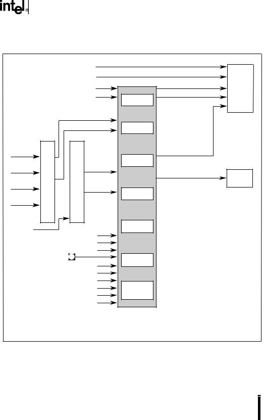
Figure 6-1. Interrupt Structure Block Diagram
6-2
STANDARD AND PTS INTERRUPTS
Interrupt Pending or PTSSRV Bit Set
|
NMI or |
Yes |
|
|
|
|
|
|
|
|
|
|
|
|
|
||
|
Stack Overflow |
|
|
|
|
|
|
|
|
|
|
|
|
|
|
|
|
|
Pending |
|
|
|
|
|
|
|
|
|
|
|
|
|
|
|
|
? |
|
|
|
|
|
|
|
|
|
|
|
|
|
|
|
||
|
|
No |
No |
|
|
|
|
|
|
|
|
|
|
|
|
|
|
|
|
|
|
|
|
|
|
|
|
|
|
|
|
|
|||
|
INT_MASK.x |
Return |
|
|
|
|
|
No |
|||||||||
= 1? |
|
|
|
|
|
|
Interrupts |
||||||||||
|
|
|
|
|
|
|
|
|
|
Enabled |
|
|
Return |
||||
|
|
Yes |
|
|
|
|
|
|
? |
|
|
|
|
|
|
||
|
PTS |
No |
|
|
|
|
|
|
Yes |
|
|
|
|
||||
|
|
|
|
|
|
|
|
|
|
|
|||||||
|
|
|
|
|
|
|
|
|
|
|
|
|
|
||||
|
|
|
|
|
|
|
|
|
|
|
|
|
|
||||
|
Enabled |
|
|
|
|
|
|
|
|
|
|
|
|
|
|
|
|
? |
|
|
|
|
|
PTSSEL.x |
|
No |
|
||||||||
|
|
Yes |
|
|
|
|
|
|
|
Bit = 0 |
|
|
|
|
|
||
|
|
|
|
|
|
|
|
|
? |
|
|
|
|
|
|
||
|
|
|
|
|
|
|
|
|
|
|
|
|
|
|
|||
|
PTSSEL.x |
No |
|
|
|
|
|
|
Yes |
|
|
|
|
||||
|
|
|
|
|
|
|
|
|
|
|
|||||||
|
|
|
|
|
|
|
|
|
|
|
|
|
|
||||
|
Bit = 1 |
|
|
|
|
|
|
|
|
|
|
|
|
|
|
|
|
? |
|
|
|
|
|
|
|
Priority |
|
|
|
|
|||||
|
|
Yes |
|
|
|
|
|
|
Resolver |
|
|
|
|
||||
|
|
|
|
|
|
|
|
|
|
|
|
||||||
|
|
|
|
|
|
|
|
|
|
|
Highest Priority Interrupt |
||||||
|
|
|
|
|
|
|
|
|
|
|
|||||||
|
Priority |
|
|
|
|
|
|
|
|
|
|
|
|
|
|
|
|
|
Resolver |
|
|
|
Yes |
|
|
|
|
|
|
No |
|||||
Highest Priority PTS Interrupt |
|
|
|
|
PTSSRV.x |
||||||||||||
|
|
|
|
|
|
|
= 1 |
|
|
|
|
|
|
||||
|
|
|
|
|
|
|
|
|
? |
|
|
|
|
|
|
||
|
Reset INT_PEND.x |
|
|
|
|
|
|
|
|
|
|
|
|
|
|
||
|
Bit |
|
|
|
|
|
|
|
|
|
|
|
|
|
|
|
|
|
|
|
|
|
Reset PTSSRV.x |
|
|
|
Reset INT_PEND.x |
|
|||||||
|
|
|
|
|
Bit |
|
|
|
|
|
|
Bit |
|
||||
|
|
|
|
|
|
|
|
|
|
|
|
|
|
|
|
|
|
|
|
|
|
|
|
|
|
|
|
|
|
|
|
|
|
|
|
|
Execute PTS Cycles |
|
|
|
|
|
|
|
|
|
|
|
|
|
|
||
|
(Microcoded) |
|
|
|
|
|
|
|
|
|
|
|
|
|
|
|
|
|
|
|
|
|
|
|
|
|
|
|
|
|
|
|
|
|
|
|
|
|
|
|
|
|
|
PUSH PC |
|
|
|
|
|||||
|
|
|
|
|
|
|
|
|
on Stack |
|
|
|
|
||||
|
Clear PTSSEL.x Bit |
|
|
|
|
|
|
|
|
|
|
|
|
|
|
||
|
|
|
|
|
|
|
|
|
|
|
|
|
|
|
|
|
|
|
|
|
|
|
|
|
LJMP to Interrupt |
|
|
|
|||||||
|
|
|
|
|
|
|
Service Routine |
|
|
|
|||||||
|
Set PTSSRV.x Bit |
|
|
|
|
|
|
|
|
|
|
|
|
|
|
||
|
|
|
|
|
|
|
|
|
|
|
|
|
|
|
|
|
|
|
|
|
|
|
|
|
Execute Interrupt |
|
|||||||||
|
|
|
|
|
|
|
Service Routine |
|
|||||||||
Request end-of-PTS interrupt |
|
|
|
|
|
|
|
|
|
|
|
|
|
||||
|
|
|
|
|
|
|
|
|
|
|
|
|
|
|
|
|
|
|
|
|
|
|
|
|
|
|
POP PC |
|
|
|
|
||||
|
|
|
|
|
|
|
|
from Stack |
|
|
|
|
|||||
|
|
|
|
|
|
|
|
|
|
|
|
|
|
|
|
|
|
|
|
|
|
|
|
|
|
|
|
Return |
|
|
|
|
A4304-03
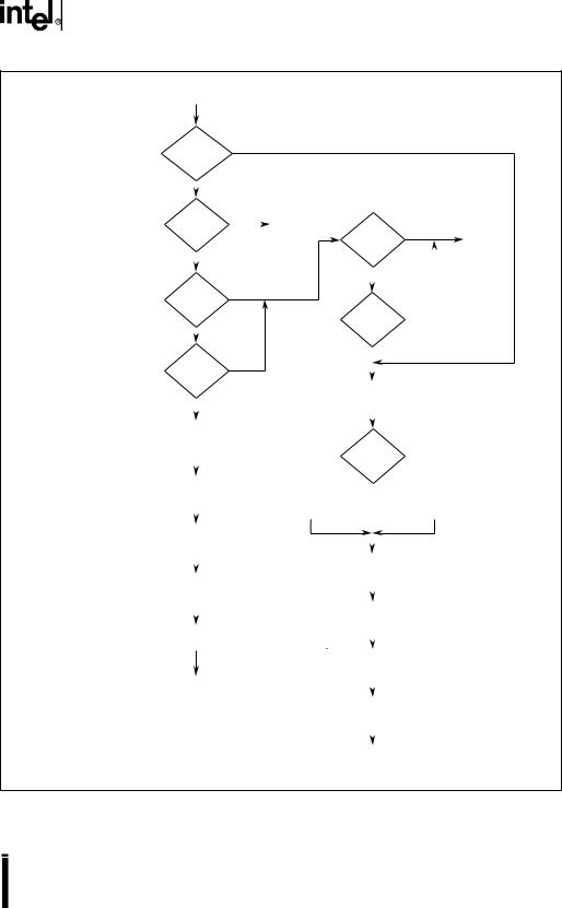
Figure 6-2. Interrupt Service Flow Diagram
6-3
8XC196EA USER’S MANUAL
6.2INTERRUPT SIGNALS AND REGISTERS
Table 6-1 describes the external interrupt signals and Table 6-2 describes the interrupt control and status registers.
|
|
Table 6-1. Interrupt Signals |
|
Interrupt |
Type |
Description |
|
Signal |
|||
|
|
||
|
|
|
|
EXTINT |
I |
External Interrupt |
|
|
|
In normal operating mode, a rising edge on EXTINT sets the EXTINT interrupt pending |
|
|
|
bit. EXTINT is sampled during phase 2 (CLKOUT high). The minimum high time is one |
|
|
|
state time. |
|
|
|
In powerdown mode, asserting the EXTINT signal for at least 50 ns causes the device |
|
|
|
to resume normal operation. The interrupt does not need to be enabled, but the pin |
|
|
|
must be configured as a special-function input. If the EXTINT interrupt is enabled, the |
|
|
|
CPU executes the interrupt service routine. Otherwise, the CPU executes the |
|
|
|
instruction that immediately follows the command that invoked the power-saving mode. |
|
|
|
In idle mode, asserting any enabled interrupt causes the device to resume normal |
|
|
|
operation. |
|
|
|
EXTINT shares a package pin with P2.2. |
|
|
|
|
|
NMI |
I |
Nonmaskable Interrupt |
|
|
|
In normal operating mode, a rising edge on NMI generates a nonmaskable interrupt. |
|
|
|
NMI has the highest priority of all prioritized interrupts. Assert NMI for greater than one |
|
|
|
state time to guarantee that it is recognized. |
|
|
|
|
Table 6-2. Interrupt and PTS Control and Status Registers
Mnemonic |
Address |
Description |
|
|
|
INT_MASK |
0008H |
Interrupt Mask Registers |
INT_MASK1 |
0013H |
The bits in these registers enable or disable each maskable |
|
|
|
|
|
interrupt (that is, each interrupt except unimplemented opcode, |
|
|
software trap, NMI, and stack overflow). |
|
|
|
INT_PEND |
0009H |
Interrupt Pending Registers |
INT_PEND1 |
0012H |
The bits in these registers are set by hardware to indicate that an |
|
|
|
|
|
interrupt is pending. |
|
|
|
PIH0_INT_MASK |
1E98H |
Peripheral Interrupt Handler (PIH) Interrupt Mask Registers |
PIH1_INT_MASK |
1EA8H |
The bits in these registers enable or disable each interrupt that is |
|
|
|
|
|
routed through the PIH. |
|
|
|
PIH0_INT_PEND |
1E9AH |
Peripheral Interrupt Handler (PIH) Interrupt Pending Registers |
PIH1_INT_PEND |
1EAAH |
The bits in these registers are set by hardware to indicate that a |
|
|
|
|
|
PIH interrupt source is pending. |
|
|
|
PIH0_PTSSEL |
1E96H |
Peripheral Interrupt Handler (PIH) PTS Select Registers |
PIH1_PTSSEL |
1EA6H |
These registers select either a PTS interrupt service request or a |
|
|
|
|
|
standard interrupt service request for each interrupt that is routed |
|
|
through the PIH. |
|
|
|
6-4